Photonics: Looking good

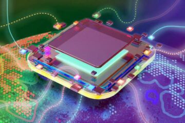
The rise of computers in past decades was made possible largely thanks to the invention of the integrated circuit, a device that combines all necessary electronic components onto a single chip. In a similar vein, the success of optical computing is largely dependent on the possibility of integrating all essential optical components onto a single chip (photonic circuit). Lim Teck Guan at the A*STAR Institute of Microelectronics and co-workers have now developed an enhanced alignment solution for photonic circuits. “Our approach offers a highly accurate, passive optical alignment solution for these devices,” says Guan.
The fabrication of photonic circuits is no easy task because there is little room for error. In order to get the best performance from these devices operating at the visible or near-infrared spectrum, various elements must be aligned with utmost precision, typically within an error of around one micrometer. Even with the slightest misalignment, a microlens, for example, might not be able to focus light into a photodetector.
The researchers came up with an alignment method that is remarkably straightforward and easy to implement. It is based on a circular through-hole with two diameters. The design of the larger hole is not critical and it can either partially or entirely accomodate the spherical lens, depending on the application requirement. A second hole in the chip is smaller than the sphere diameter so that if the lens is pressed against the opening the sphere will automatically be aligned in its center. In this way, light from underneath the chip is guided through the lens and the second hole, and on to a photodetector that is placed directly above.
This guided assembly scheme makes it easy to fabricate more complex photonic circuits, once the spherical lenses are integrated with the layer containing the through-holes. Electronic circuits of virtually any complexity can be placed on the chip with high accuracy, so that they align perfectly with the optical beam shone through the lens. The measured efficiencies of the light coupling between the different components on the chip are promising and demonstrate light propagation with few losses.
In the current assembly, a laser is placed on a chip and through a combination of mirrors and microsphere lenses, the light is guided across the chip to a photodetector. However, the researchers have already set their sights on the advantages of further integration. “In future, we might come up with more complex circuits,” suggests Guan. “These devices could lead to applications including high-speed, high-bandwidth integrated photonic circuits, particularly if we can integrate conventional silicon electronics with photonic functionality.”
References
Guan, L. T. et al. Integrated optical carrier for optical/electrical interconnect. IEEE Transactions on Components, Packaging, and Manufacturing Technology 1, 125–132 (2011).
Media Contact
All latest news from the category: Power and Electrical Engineering
This topic covers issues related to energy generation, conversion, transportation and consumption and how the industry is addressing the challenge of energy efficiency in general.
innovations-report provides in-depth and informative reports and articles on subjects ranging from wind energy, fuel cell technology, solar energy, geothermal energy, petroleum, gas, nuclear engineering, alternative energy and energy efficiency to fusion, hydrogen and superconductor technologies.
Newest articles

A universal framework for spatial biology
SpatialData is a freely accessible tool to unify and integrate data from different omics technologies accounting for spatial information, which can provide holistic insights into health and disease. Biological processes…

How complex biological processes arise
A $20 million grant from the U.S. National Science Foundation (NSF) will support the establishment and operation of the National Synthesis Center for Emergence in the Molecular and Cellular Sciences (NCEMS) at…

Airborne single-photon lidar system achieves high-resolution 3D imaging
Compact, low-power system opens doors for photon-efficient drone and satellite-based environmental monitoring and mapping. Researchers have developed a compact and lightweight single-photon airborne lidar system that can acquire high-resolution 3D…


