Transparent emissive microdisplays
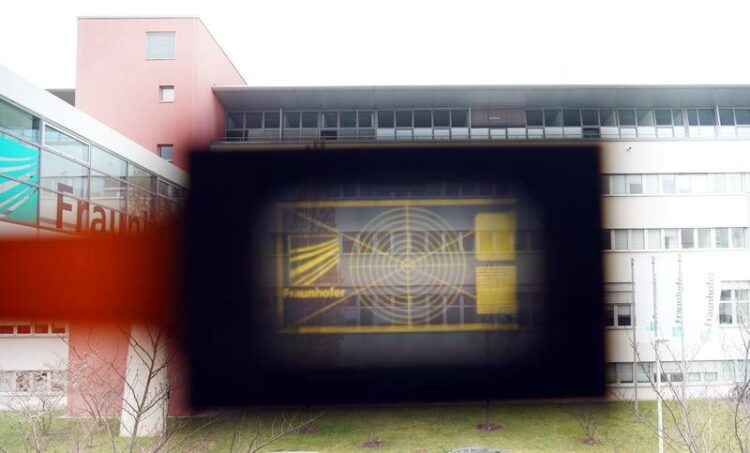
Transparent OLED microdisplay
©Fraunhofer IPMS
… for ultra-light and compact augmented reality systems.
As part of the HOT project (High-performance transparent and flexible microelectronics for photonic and optical applications), scientists from the Fraunhofer Institute for Photonic Microsystems IPMS have developed a semi-transparent microdisplay. This microdisplay is significantly lighter than conventional combiner-based optical see-through near-to-eye systems and offers high resolution. The microdisplay will be presented at the SID Display Week 2024 in San Jose, USA, at the German Pavilion, booth number 1124.
In today’s time, more and more augmented-reality (AR) glasses and see-through systems with different application areas are entering the market. To increase the acceptance of these devices and improve wearing comfort, it is important that they are lightweight and easy to use. For mobile consumer electronics devices, the key acceptance criteria are form factor or compactness (volume, weight), battery life, connectivity, app ecosystem, and cost.
OLED microdisplays are ideal as image generators for virtual-reality (VR), augmented-reality (AR), and mixed-reality (MR) applications, due to their high resolution and technological level/maturity. However, these microdisplays are typically not transparent due to their silicon-based technology. Therefore, a complex optical system is required for use in see-through data glasses and similar devices, which allows the combination of real and virtual images (optical combiner). This has significant implications on the weight, size, and optical efficiency of the entire glasses. Current optical see-through near-to-eye displays (NTE) in augmented-reality devices attempt to solve the form factor problem through various technical approaches, such as coupling images from non-transparent image sources into waveguide or fold element optics.
The scientists at the Fraunhofer Institute for Photonic Microsystems IPMS have years of experience in developing innovative designs for novel microdisplays and possess a globally unique expertise in this field. Thanks to their newly developed semi-transparent OLED-on-silicon microdisplay technology, completely new possibilities for optical design of slim, near-eye optics are being opened up.
Philipp Wartenberg, Group manager IC and System Design at Fraunhofer IPMS, explains: “Modern and advanced silicon CMOS processes are increasingly being applied to silicon-on-insulator (SOI) wafers. This wafer technology can be used for implementation of very thin circuitry layers. With the help of a specific IC design and an appropriate process flow which enables transfer on a glass wafer semi-transparent microdisplays are possible.”
Depending on the design approach, microoptics can already be directly integrated on the chip. The transparent microdisplay itself becomes an optical combiner element, significantly reducing the size of the optical system and improving optical efficiency significantly. Further internal technology studies indicate that transparencies of over 50% are achievable.
The scientists are pleased with the successful first technology demonstrator of the transparent microdisplay. They continue to work on increasing transparency and are ready for customer- and application-specific developments to bring this novel technology to market readiness.
About the HOT project (High-performance transparent and flexible microelectronics for photonic and optical applications):
This work was funded within a Fraunhofer internal program under grant number MAVO 840092. In addition, the scientists were supported by Fraunhofer IOF in the field of microoptics.
About Fraunhofer IPMS
Fraunhofer IPMS is one of the leading international research and development service providers for electronic and photonic microsystems in the application fields of intelligent industrial solutions and manufacturing, medical technology and health, and mobility. In two state-of-the-art clean rooms and with a total of four development sites in Dresden, Cottbus and Erfurt, the institute develops innovative MEMS components and microelectronic devices on 200 mm and 300 mm wafers. Services range from consulting and process development to pilot production.
Media Contact
All latest news from the category: Power and Electrical Engineering
This topic covers issues related to energy generation, conversion, transportation and consumption and how the industry is addressing the challenge of energy efficiency in general.
innovations-report provides in-depth and informative reports and articles on subjects ranging from wind energy, fuel cell technology, solar energy, geothermal energy, petroleum, gas, nuclear engineering, alternative energy and energy efficiency to fusion, hydrogen and superconductor technologies.


Newest articles

Faster, more energy-efficient way to manufacture an industrially important chemical
Zirconium combined with silicon nitride enhances the conversion of propane — present in natural gas — needed to create in-demand plastic, polypropylene. Polypropylene is a common type of plastic found…

Energy planning in Ghana as a role model for the world
Improving the resilience of energy systems in the Global South. What criteria should we use to better plan for resilient energy systems? How do socio-economic, technical and climate change related…

Artificial blood vessels could improve heart bypass outcomes
Artificial blood vessels could improve heart bypass outcomes. 3D-printed blood vessels, which closely mimic the properties of human veins, could transform the treatment of cardiovascular diseases. Strong, flexible, gel-like tubes…

