Electronics from the printer
Televisions have changed dramatically: While bulky TV sets dominated our living rooms until just a few years ago, the screens are now so flat that they can easily be hung on the wall.
A close look at the inside of these devices will reveal fine conductor paths and transistors that supply the electricity needed to switch the pixels on the screen on and off. These circuits are manufactured layer by layer, usually by photolithography. The materials are deposited onto the entire surface of a substrate and covered with photoresist, which is exposed to light at specific points using a mask.
The exposed photoresist alters its chemical properties: It becomes soluble and can be easily removed. The layer to be structured returns to the surface and can be etched away. However, the parts of the layer still covered with photoresist remain intact. One major disadvantage of this process is that a large fraction of the deposited material is not used. A more cost-efficient and resource-saving method is to deposit the material by printing only in places where it will actually be needed later.
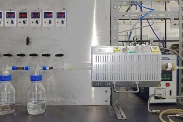
Printed electronics already exist in the form of conductor paths and devices made from polymers. However, their electrical properties cannot compete with those of inorganic materials. The charge carriers in the polymers travel more slowly, with the result that a printed RFID tag, for example, will have a shorter transmission range than a conventional one. Moreover, polymers tend to react more sensitively to moisture and UV light. Researchers at the Fraunhofer Institute of Integrated Systems and Device Technology IISB in Erlangen have now commissioned a process line in which electron devices can be printed from inorganic materials using an ink jet similar to those in any office printer. “We use ink made of nanoparticles and add a stabilizer so that the particles can be easily processed and do not clump together,” says IISB group manager Dr. Michael Jank.
The nano ink has passed the first printing tests and Jank hopes that the researchers will be able to print circuits performing simple functions in about a year’s time. “We expect printed products to cost around 50 percent less than silicon-based ones in the case of simple circuits,” he says. “Printed RFID tags should then be cheap enough to be attached to the packaging of low-cost products such as yogurts, where they can then monitor the temperature, and store and transmit data.”
Media Contact
All latest news from the category: Power and Electrical Engineering
This topic covers issues related to energy generation, conversion, transportation and consumption and how the industry is addressing the challenge of energy efficiency in general.
innovations-report provides in-depth and informative reports and articles on subjects ranging from wind energy, fuel cell technology, solar energy, geothermal energy, petroleum, gas, nuclear engineering, alternative energy and energy efficiency to fusion, hydrogen and superconductor technologies.


Newest articles
Recovering phosphorus from sewage sludge ash
Chemical and heat treatment of sewage sludge can recover phosphorus in a process that could help address the problem of diminishing supplies of phosphorus ores. Valuable supplies of phosphorus could…
Efficient, sustainable and cost-effective hybrid energy storage system for modern power grids
EU project HyFlow: Over three years of research, the consortium of the EU project HyFlow has successfully developed a highly efficient, sustainable, and cost-effective hybrid energy storage system (HESS) that…

After 25 years, researchers uncover genetic cause of rare neurological disease
Some families call it a trial of faith. Others just call it a curse. The progressive neurological disease known as spinocerebellar ataxia 4 (SCA4) is a rare condition, but its…

