Ultra-large single-crystal WS2 monolayer
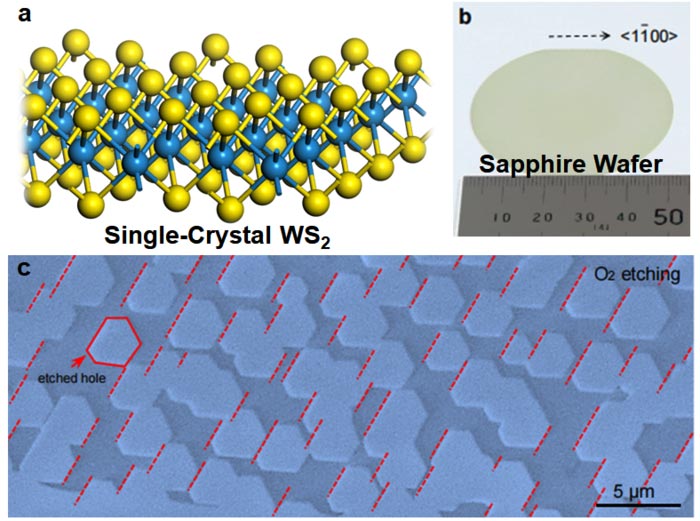
a: Single-crystal WS2; b: Sapphire wafer used in industry is a single-crystal; c: Experimental images about the WS2 films on sapphire wafer after O2 etching.
Credit: Institute for Basic Science
New technique opens a possibility to replace silicon with 2D materials in semiconducting technology.
As silicon based semiconducting technology is approaching the limit of its performance, new materials that may replace or partially replace silicon in technology is highly desired. Recently, the emergence of graphene and other two-dimensional (2D) materials offers a new platform for building next generation semiconducting technology. Among them, transition metal dichalcogenides (TMDs), such as MoS2, WS2, MoSe2, WSe2, as most appealing 2D semiconductors.
A prerequisite of building ultra-large-scale high-performance semiconducting circuits is that the base materials must be a single-crystal of wafer-scale, just like the silicon wafer used today. Although great efforts have been dedicated to the growth of wafer-scale single-crystals of TMDs, the success was very limited until now.
Distinguished Professor Feng Ding and his research team from the Center for Multidimensional CarbonMaterials (CMCM), within the Institute for Basic Science (IBS) at UNIST, in cooperation with researcher at Peking University (PKU), Beijing Institute of Technology, and Fudan University, reported the direct growth of 2-inch single-crystal WS2 monolayer films very recently. Besides the WS2, the research team also demonstrated the growth of single-crystal MoS2, WSe2, and MoSe2 in wafer scale as well.
Credit: Institute for Basic Science
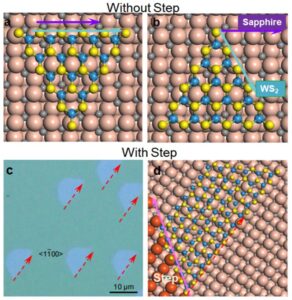
The key technology of epitaxially grown a large sing-crystal is to ensure that all small single-crystal grown on a substrate are uniformly aligned. Because TMDs has non-centrosymmetric structure or the mirror image of a TMD with respect to an edge of it has opposite alignment, we must break such a symmetry by carefully design the substrate. Based on theoretical calculations, the authors proposed a mechanisms of “dual-coupling-guided epitaxy growth” for experimental design. The WS2-sapphire plane interaction as the first driving force, leading to two preferred antiparallel orientations of the WS2 islands. The coupling between WS2 and sapphire step-edge is the second driving force and it will break the degeneracy of the two antiparallel orientations. Then all the TMD single crystals grown on a substrate with step edges are all unidirectional aligned and finally, the coalescence of these small single-crystals leads to a large single-crystal of the same size of the substrate.
“This new dual-coupling epitaxy growth mechanism is new for controllable materials growth. In principle, it allows us realize to grow all 2D materials into large-area single crystals if proper substrate was found.” Says Dr. Ting Cheng, the co-first author of the study. “We have considered how to choose proper substrates theoretically. First, the substrate should have a low symmetry and, secondly, more step edges are preferred.” emphasizes Professor Feng Ding, the corresponding author of the study.
“This is a major step forward in the area of 2D materials based device. As the successful growth of wafer-scale single-crystal 2D TMDs on insulators beyond graphene and hBN on transition metal substrates, our study provide the required keystone of 2D semiconductors in high-end applications of electronic and optical devices,” explains professor Feng Ding.
Journal: Nature Nanotechnology
DOI: 10.1038/s41565-021-01004-0
Method of Research: Experimental study
Subject of Research: Not applicable
Article Title: Dual-coupling-guided epitaxial growth of wafer-scale single-crystal WS2 monolayer on vicinal a-plane sapphire
Article Publication Date: 15-Nov-2021
Media Contact
William Suh
Institute for Basic Science
willisuh@ibs.re.kr
Office: 82-010-379-37830
All latest news from the category: Materials Sciences
Materials management deals with the research, development, manufacturing and processing of raw and industrial materials. Key aspects here are biological and medical issues, which play an increasingly important role in this field.
innovations-report offers in-depth articles related to the development and application of materials and the structure and properties of new materials.


Newest articles

High-energy-density aqueous battery based on halogen multi-electron transfer
Traditional non-aqueous lithium-ion batteries have a high energy density, but their safety is compromised due to the flammable organic electrolytes they utilize. Aqueous batteries use water as the solvent for…

First-ever combined heart pump and pig kidney transplant
…gives new hope to patient with terminal illness. Surgeons at NYU Langone Health performed the first-ever combined mechanical heart pump and gene-edited pig kidney transplant surgery in a 54-year-old woman…

Biophysics: Testing how well biomarkers work
LMU researchers have developed a method to determine how reliably target proteins can be labeled using super-resolution fluorescence microscopy. Modern microscopy techniques make it possible to examine the inner workings…

