Double-layer capping solves two problems

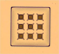
An optical image of a 400-by-400-micrometer, thin-film MEMS encapsulation developed using the new double-layer capping technique. The smaller square caps sit on top of holes, allowing access to the cavity below while protecting the devices within.<br><br>Reproduced from Ref. 1 © 2013 IOP Publishing
Continual downsizing of technology means that researchers have to develop ever more ingenious methods of packaging and protecting their tiny devices. Jae-Wung Lee and co-workers at the A*STAR Institute of Microelectronics, Singapore, are at the forefront of efforts to develop safe but functional encasements for microelectromechanical systems (MEMS), such as sensors, switches or radio filters.
“MEMS devices need certain ambient conditions to operate properly and have fragile hanging structures that must be protected,” says Lee. “We developed a new thin-film encapsulation (TFE) technique to meet these two requirements.”
During TFE, a MEMS device is embedded in a ‘sacrificial layer’ of one material before adding a ‘cap layer’ of another type of material. By leaving some access channels in the cap layer, researchers can pipe in a chemical that reacts with and removes the sacrificial layer, leaving the MEMS device in a cavity protected by the cap layer.
Compared with other encasement methods, TFE can be performed cheaply using the same techniques that are used to build MEMS devices, and it produces less bulky packaging. However, previous attempts at TFE have suffered from two problems: depending on the design of the access holes in the cap layer, removing the sacrificial layer can be time consuming, and mass loading can damage moving components, such as resonators, in MEMS devices.
“Solving both these issues simultaneously is difficult because one can become severe when the other is solved,” says Lee. “We proposed fabricating the cap layer on two levels.”
The team’s design involves making a grid of square holes in the lower cap layer. A secondary square layer with four legs is deposited on top of each hole, leaving sideways access gaps underneath, rather like a chimney cap. These caps allow access for removing the sacrificial layer while protecting the device beneath from mass loading.
The researchers tested their idea using silicon oxide as the sacrificial layer and aluminum nitride for the cap layers. They were able to remove the silicon oxide using an acid vapor in just 20 minutes, compared to 8 hours for previous designs. The result was a strong, free-standing cap with a 3-micrometer-thick cavity underneath.
Lee and co-workers state that their TFE cavity design could be built using other materials and may find application beyond MEMS, for instance in microbiology. “Electrodes embedded in a TFE cavity could be used to apply electrostatic forces to biomolecules or even act as a microheater,” says Le
The A*STAR-affiliated researchers contributing to this research are from the Institute of Microelectronics.
Journal information
Lee, J.-W., Sharma, J., Singh, N. and Kwong, D.-L. Development and evaluation of a two-level functional structure for the thin film encapsulation. Journal of Micromechanics and Microengineering 23, 075013 (2013).
Media Contact
All latest news from the category: Power and Electrical Engineering
This topic covers issues related to energy generation, conversion, transportation and consumption and how the industry is addressing the challenge of energy efficiency in general.
innovations-report provides in-depth and informative reports and articles on subjects ranging from wind energy, fuel cell technology, solar energy, geothermal energy, petroleum, gas, nuclear engineering, alternative energy and energy efficiency to fusion, hydrogen and superconductor technologies.
Newest articles

A universal framework for spatial biology
SpatialData is a freely accessible tool to unify and integrate data from different omics technologies accounting for spatial information, which can provide holistic insights into health and disease. Biological processes…

How complex biological processes arise
A $20 million grant from the U.S. National Science Foundation (NSF) will support the establishment and operation of the National Synthesis Center for Emergence in the Molecular and Cellular Sciences (NCEMS) at…

Airborne single-photon lidar system achieves high-resolution 3D imaging
Compact, low-power system opens doors for photon-efficient drone and satellite-based environmental monitoring and mapping. Researchers have developed a compact and lightweight single-photon airborne lidar system that can acquire high-resolution 3D…


