High Speed Processing on Large Wafers
The new system concept enables solar cell manufacturers to perform laser processing at the highest speed without having to compromise on structure size or processing area.
Fraunhofer ISE
… with Newly Developed On-the-Fly Laser Equipment.
In order to be able to manufacture more efficient solar modules, the photovoltaic industry is increasingly switching its production to larger wafer formats. Being able to guarantee the production of these solar cells with an edge length of up to 210 millimeters with consistent quality and cycle rate poses new challenges for equipment manufacturers. A research team at the Fraunhofer Institute for Solar Energy System ISE has now succeeded in implementing a novel system concept, whereby large-format solar cells are continually processed as they move at high speed under the laser scanner.
The new system for solar cell processing can laser half a million contact openings per second and has an effective throughput of over 15,000 solar wafers per hour.
Visitors to LASER World of PHOTONICS 2022 (April 26-29, Messe München) can learn more about the system concept at the Fraunhofer booth 441 in Hall A6.
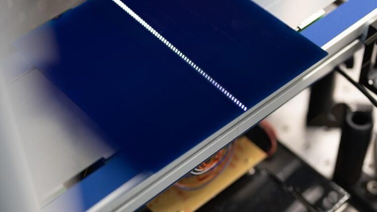
To produce common Passivated Emitter and Rear Cell (PERC) solar cells, laser pulses are used to locally open thin insulating layers for electrical contacting. With the new concept, solar cell manufacturers can move large-area formats up to an edge length of 210 millimeters. According to forecasts of the International Technology Roadmap for Photovoltaics 2022, half of the solar cells produced this year will have an edge length longer than 180mm. At present, it is not possible to achieve these formats using standard laser processing systems without making compromises: A larger processing area means either a reduction in the traversing speed of the laser beam or applying larger structure sizes, which results respectively in either a loss in throughput or in quality. In this regard, the throughput of commercially available systems used today for solar cell structuring and metallization already is a limiting factor.
The new Fraunhofer ISE concept, on the other hand, is suitable for implementing large-area wafer formats such as M12 and G12, even with high throughput and small structure sizes. At the heart of the new system is the polygon scan technology from project partner MOEWE Optical Solutions GmbH, in which a high-speed mirror wheel moves the laser beam over the sample at over 3,000 kilometers per hour. This is about 20 times faster than the galvanometer scanners commonly used today. “To tap the potential of ultrafast scanners and lasers, we developed sensor technology designed specifically for the new system in order to achieve the required positioning accuracy despite the high speed,” says Dr. Fabian Meyer, team leader of Laser System Development at Fraunhofer ISE. With 15,000 solar wafers per hour, the throughput of the new system is significantly higher than the current industry standard of 7000 per hour. In addition, Meyer’s team was able to demonstrate that PERC solar cells processed with the demonstrator system have the same high efficiency as cells produced according to the current industry standard.
Because of the low operating costs of laser processing, the researchers expect significant cost benefits from their high-throughput technology. “The results of the research team therefore make an important contribution to increasing productivity and reducing costs in solar cell production,” says Dr. Ralf Preu, division director of Photovoltaic Production Technology at Fraunhofer ISE. “The demonstrated system concept is a groundbreaking development for the improvement of structuring processes in the photovoltaic production chain.”
Wissenschaftliche Ansprechpartner:
Dr. Fabian Meyer, Laser System Development: fabian.meyer@ise.fraunhofer.de
Weitere Informationen:
https://ise.link/laser-otf Research on Laser Technologies at Fraunhofer ISE
Media Contact
All latest news from the category: Process Engineering
This special field revolves around processes for modifying material properties (milling, cooling), composition (filtration, distillation) and type (oxidation, hydration).
Valuable information is available on a broad range of technologies including material separation, laser processes, measuring techniques and robot engineering in addition to testing methods and coating and materials analysis processes.


Newest articles

A universal framework for spatial biology
SpatialData is a freely accessible tool to unify and integrate data from different omics technologies accounting for spatial information, which can provide holistic insights into health and disease. Biological processes…

How complex biological processes arise
A $20 million grant from the U.S. National Science Foundation (NSF) will support the establishment and operation of the National Synthesis Center for Emergence in the Molecular and Cellular Sciences (NCEMS) at…

Airborne single-photon lidar system achieves high-resolution 3D imaging
Compact, low-power system opens doors for photon-efficient drone and satellite-based environmental monitoring and mapping. Researchers have developed a compact and lightweight single-photon airborne lidar system that can acquire high-resolution 3D…

