Silicon nanopillars for quantum communication
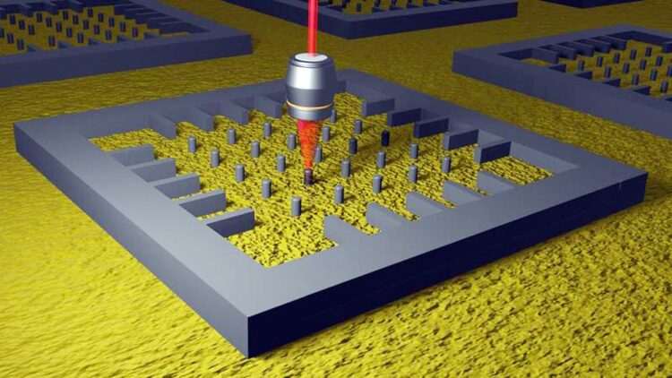
The researchers use an objective lens to test the light output from an array of silicon nanopillars on a chip.
(c) HZDR / Juan Baratech
New production technology opens the way to quantum light sources with fiber optic compatibility.
Across the world, specialists are working on implementing quantum information technologies. One important path involves light: Looking ahead, single light packages, also known as light quanta or photons, could transmit data that is both coded and effectively tap proof. To this end, new photon sources are required that emit single light quanta in a controlled fashion – and on demand. Only recently has it been discovered that silicon can host sources of single-photons with properties suitable for quantum communication. So far, however, no-one has known how to integrate the sources into modern photonic circuits.
For the first time, a team led by the Helmholtz-Zentrum Dresden-Rossendorf (HZDR) has now presented an appropriate production technology using silicon nanopillars: a chemical etching method followed by ion bombardment (DOI: 10.1063/5.0094715).
“Silicon and single-photon sources in the telecommunication field have long been the missing link in speeding up the development of quantum communication by optical fibers. Now we have created the necessary preconditions for it,” explains Dr. Yonder Berencén of HZDR’s Institute of Ion Beam Physics and Materials Research who led the current study. Although single-photon sources have been fabricated in materials like diamonds, only silicon-based sources generate light particles at the right wavelength to proliferate in optical fibers – a considerable advantage for practical purposes.
The researchers achieved this technical breakthrough by choosing a wet etching technique – what is known as MacEtch (metal-assisted chemical etching) – rather than the conventional dry etching techniques for processing the silicon on a chip. These standard methods, which allow the creation of silicon photonic structures, use highly reactive ions. These ions induce light-emitting defects caused by the radiation damage in the silicon. However, they are randomly distributed and overlay the desired optical signal with noise. Metal-assisted chemical etching, on the other hand does not generate these defects – instead, the material is etched away chemically under a kind of metallic mask.
The goal: single photon sources compatible with the fiber-optic network
Using the MacEtch method, researchers initially fabricated the simplest form of a potential light wave-guiding structure: silicon nanopillars on a chip. They then bombarded the finished nanopillars with carbon ions, just as they would with a massive silicon block, and thus generated photon sources embedded in the pillars. Employing the new etching technique means the size, spacing, and surface density of the nanopillars can be precisely controlled and adjusted to be compatible with modern photonic circuits. Per square millimeter chip, thousands of silicon nanopillars conduct and bundle the light from the sources by directing it vertically through the pillars.
The researchers varied the diameter of the pillars because “we had hoped this would mean we could perform single defect creation on thin pillars and actually generate a single photon source per pillar” explains Berencén. “It didn’t work perfectly the first time. By comparison, even for the thinnest pillars, the dose of our carbon bombardment was too high. But now it’s just a short step to single photon sources.”
A step on which the team is already working intensively because the new technique has also unleashed something of a race for future applications. “My dream is to integrate all the elementary building blocks, from a single photon source via photonic elements through to a single photon detector, on one single chip and then connect lots of chips via commercial optical fibers to form a modular quantum network,” says Berencén.
Wissenschaftliche Ansprechpartner:
Dr. Yonder Berencén
Institute of Ion Beam Physics and Materials Research at HZDR
Phone: +49 351 260 3137 | Email: y.berencen@hzdr.de
Originalpublikation:
M. Hollenbach, N. S. Jagtap, C. Fowley, J. Baratech, V. Guardia-Arce, U. Kentsch, A. Eichler-Volf, N. V. Abrosimov, A. Erbe, C.Shin, H. Kim, M. Helm, W. Lee, G. V. Astakhov and Y. Berencén: Metal-assisted chemically etched silicon nanopillars hosting telecom photon emitters, Journal of Applied Physics, 2022 (DOI: 10.1063/5.0094715)
M. Hollenbach, Y. Berencén, U. Kentsch, M. Helm, G. Astakhov: Engineering telecom single-photon emitters in silicon for scalable quantum photonics, Optics Express, 2020 (DOI: 10.1364/OE.397377)
Media Contact
All latest news from the category: Information Technology
Here you can find a summary of innovations in the fields of information and data processing and up-to-date developments on IT equipment and hardware.
This area covers topics such as IT services, IT architectures, IT management and telecommunications.


Newest articles

High-energy-density aqueous battery based on halogen multi-electron transfer
Traditional non-aqueous lithium-ion batteries have a high energy density, but their safety is compromised due to the flammable organic electrolytes they utilize. Aqueous batteries use water as the solvent for…

First-ever combined heart pump and pig kidney transplant
…gives new hope to patient with terminal illness. Surgeons at NYU Langone Health performed the first-ever combined mechanical heart pump and gene-edited pig kidney transplant surgery in a 54-year-old woman…

Biophysics: Testing how well biomarkers work
LMU researchers have developed a method to determine how reliably target proteins can be labeled using super-resolution fluorescence microscopy. Modern microscopy techniques make it possible to examine the inner workings…

