Microchips: Smaller, more powerful and unrivaled
Smaller, faster and more powerful: unrivaled process for manufacturing microchips with process sizes of less than 10 nm.
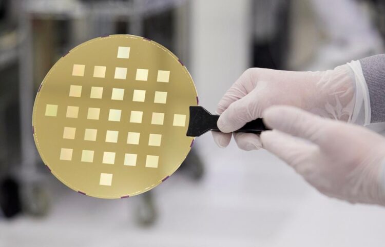
© Fraunhofer / Piotr Banczerowski
The evolution of microchips seemed to have reached its limits, as far as their size is concerned. Nevertheless, it is crucial that these small components be-come even smaller and more powerful so that many devices — including smartphones — can be developed even further. The Fraunhofer Institute for Silicon Technology ISIT in Itzehoe and IMS Nanofabrication GmbH have now succeeded in pushing the existing boundaries when it comes to MEMS pro-cessing of a microsystem switching element which is at the core of an elec-tron beam mask writer — a crucial piece of equipment in the production of the latest generation of microchips. Their efforts have earned them the 2021 Joseph von Fraunhofer Prize.
The continuous development of smartphones and other electronic devices can be summed up as “smaller, faster, more powerful.” At the core of these devices are microchips that also need to become smaller and better as part of this development. Good progress has been made in this area in the past, but many manufacturing technologies are now reaching their limits.
Only solution in the world
The only solution in the world that has shifted the existing limits stems from an in-novative piece of technology: the electron multi-beam mask writer, developed by Vienna-based IMS Nanofabrication GmbH. The key element in this device comes from the Fraunhofer Institute for Silicon Technology ISIT. “Previously, it was only possible to achieve process sizes of just under ten nanometers on the chips — an atom is 0.1 nanometers — but the new manufacturing method makes process sizes of seven nanometers and less a possibility,” says Martin Witt from Fraunhofer ISIT.
This is unrivaled around the world, meaning the electron multi-beam mask writer is currently the only technology that enables further miniaturization of the chips. The fact that “this technology enabled IMS Nanofabrication GmbH to achieve its mar-ket-leading position” was also praised by the jury for the 2021 Joseph von Fraunho-fer Prize, who gave the award to Michael Kampmann and Martin Witt from Fraun-hofer ISIT and Dr. Jacqueline Atanelov from IMS GmbH.
In conventional chip production, a wafer of the semiconductor material silicon is coated evenly with photoresist, which is hardened by exposing it to targeted light. The areas that are not hardened are removed and the silicon is processed at the exposed areas. The hardened part of the photoresist is then also removed and the process starts all over again. In this way, the chip is created layer by layer — for complex chips, up to 70 light exposure stages are necessary. To ensure the light is targeted to where the photoresist needs to be hardened while leaving the other areas in the dark, various masks are used. These are produced in a similar way to the chips, but in this case an electron beam is used to harden the photoresist.
What is the key feature of this new method? “Instead of writing the mask struc-tures on the electron-sensitive photoresist with a single beam, we use 512 times 512 beams, so more than 262,000 beams,” explains Kampmann. This is made possi-ble by a micro-electromechanical system (MEMS) switching element from Fraunho-fer ISIT, which essentially forms the core of the new multi-beam mask writer. In simple terms, this microsystem switching element is like a membrane with more than 262,000 openings that allow the electron beams through. But unlike jets of water from a shower head, these beams do not run in parallel. Instead, they can be individually controlled and redirected by special control electrodes.
Unrivaled
“The electron multi-beam mask writer allows us to create complex structures in high quality and resolution in just a few hours,” adds Atanelov. There is currently no technology to rival the innovative electron multi-beam mask writer. As a result, there is significant demand in the market and the devices are bringing in an annual revenue of $400 million for IMS. The impact can be seen at Fraunhofer ISIT as well: Industry revenue is now well in excess of one million euros a year. This prizewinning technology is not only enabling further miniaturization to be achieved, but is also bringing about outstanding commercial success.
Originalpublikation:
https://www.fraunhofer.de/en/press/research-news/2021/may-2021/smaller-more-powe…
Weitere Informationen:
https://www.fraunhofer.de/en/press/research-news/2021/may-2021/smaller-more-powe…
Media Contact
All latest news from the category: Information Technology
Here you can find a summary of innovations in the fields of information and data processing and up-to-date developments on IT equipment and hardware.
This area covers topics such as IT services, IT architectures, IT management and telecommunications.


Newest articles

A universal framework for spatial biology
SpatialData is a freely accessible tool to unify and integrate data from different omics technologies accounting for spatial information, which can provide holistic insights into health and disease. Biological processes…

How complex biological processes arise
A $20 million grant from the U.S. National Science Foundation (NSF) will support the establishment and operation of the National Synthesis Center for Emergence in the Molecular and Cellular Sciences (NCEMS) at…

Airborne single-photon lidar system achieves high-resolution 3D imaging
Compact, low-power system opens doors for photon-efficient drone and satellite-based environmental monitoring and mapping. Researchers have developed a compact and lightweight single-photon airborne lidar system that can acquire high-resolution 3D…

