Lithography-free photonic chip offers speed and accuracy for artificial intelligence
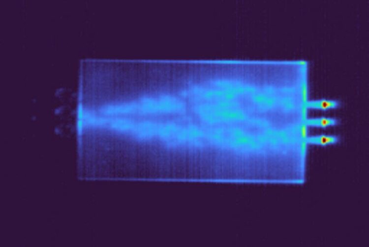
Light creates a computational network on a piece of unpatterned semiconductor wafer. The Feng Lab team’s achievement allows for on-chip processing with no lithographic etching, signaling cheaper and easier manufacturing and superior accuracy for AI applications.
Credit: University of Pennsylvania
Photonic chips have revolutionized data-heavy technologies. On their own or in concert with traditional electronic circuits, these laser-powered devices send and process information at the speed of light, making them a promising solution for artificial intelligence’s data-hungry applications.
In addition to their incomparable speed, photonic circuits use significantly less energy than electronic ones. Electrons move relatively slowly through hardware, colliding with other particles and generating heat, while photons flow without losing energy, generating no heat at all. Unburdened by the energy loss inherent in electronics, integrated photonics are poised to play a leading role in sustainable computing.
Photonics and electronics draw on separate areas of science and use distinct architectural structures. Both, however, rely on lithography to define their circuit elements and connect them sequentially. While photonic chips don’t make use of the transistors that populate electronic chips’ ever-shrinking and increasingly layered grooves, their complex lithographic patterning guides laser beams through a coherent circuit to form a photonic network that can perform computational algorithms.
But now, for the first time, researchers at the University of Pennsylvania School of Engineering and Applied Science have created a photonic device that provides programmable on-chip information processing without lithography, offering the speed of photonics augmented by superior accuracy and flexibility for AI applications.
Achieving unparalleled control of light, this device consists of spatially distributed optical gain and loss. Lasers cast light directly on a semiconductor wafer, without the need for defined lithographic pathways.
Liang Feng, Professor in the Departments of Materials Science and Engineering (MSE) and Electrical Systems and Engineering (ESE), along with Ph.D. student Tianwei Wu (MSE) and postdoctoral fellows Zihe Gao and Marco Menarini (ESE), introduced the microchip in a recent study published in Nature Photonics.
Silicon-based electronic systems have transformed the computational landscape. But they have clear limitations: they are slow in processing signal, they work through data serially and not in parallel, and they can only be miniaturized to a certain extent. Photonics is one of the most promising alternatives because it can overcome all these shortcomings.
“But photonic chips intended for machine learning applications face the obstacles of an intricate fabrication process where lithographic patterning is fixed, limited in reprogrammability, subject to error or damage and expensive,” says Feng. “By removing the need for lithography, we are creating a new paradigm. Our chip overcomes those obstacles and offers improved accuracy and ultimate reconfigurability given the elimination of all kinds of constraints from predefined features.”
Without lithography, these chips become adaptable data-processing powerhouses. Because patterns are not pre-defined and etched in, the device is intrinsically free of defects. Perhaps more impressively, the lack of lithography renders the microchip impressively reprogrammable, able to tailor its laser-cast patterns for optimal performance, be the task simple (few inputs, small datasets) or complex (many inputs, large datasets).
In other words, the intricacy or minimalism of the device is a sort of living thing, adaptable in ways no etched microchip could be.
“What we have here is something incredibly simple,” says Wu. “We can build and use it very quickly. We can integrate it easily with classical electronics. And we can reprogram it, changing the laser patterns on the fly to achieve real-time reconfigurable computing for on-chip training of an AI network.”
An unassuming slab of semiconductor, the device couldn’t be simpler. It’s the manipulation of this slab’s material properties that is the key to research team’s breakthrough in projecting lasers into dynamically programmable patterns to reconfigure the computing functions of the photonic information processor.
This ultimate reconfigurability is critical for real-time machine learning and AI.
“The interesting part,” says Menarini, “is how we are controlling the light. Conventional photonic chips are technologies based on passive material, meaning its material scatters light, bouncing it back and forth. Our material is active. The beam of pumping light modifies the material such that when the signal beam arrives, it can release energy and increase the amplitude of signals.”
“This active nature is the key to this science, and the solution required to achieve our lithography-free technology,” adds Gao. “We can use it to reroute optical signals and program optical information processing on-chip.”
Feng compares the technology to an artistic tool, a pen for drawing pictures on a blank page.
“What we have achieved is exactly the same: pumping light is our pen to draw the photonic computational network (the picture) on a piece of unpatterned semiconductor wafer (the blank page).”
But unlike indelible lines of ink, these beams of light can be drawn and redrawn, their patterns tracing innumerable paths to the future.
Journal: Nature Photonics
DOI: 10.1038/s41566-023-01205-0
Article Title: Lithography-free reconfigurable integrated photonic processor
Article Publication Date: 27-Apr-2023
Media Contact
All latest news from the category: Information Technology
Here you can find a summary of innovations in the fields of information and data processing and up-to-date developments on IT equipment and hardware.
This area covers topics such as IT services, IT architectures, IT management and telecommunications.


Newest articles

Faster, more energy-efficient way to manufacture an industrially important chemical
Zirconium combined with silicon nitride enhances the conversion of propane — present in natural gas — needed to create in-demand plastic, polypropylene. Polypropylene is a common type of plastic found…

Energy planning in Ghana as a role model for the world
Improving the resilience of energy systems in the Global South. What criteria should we use to better plan for resilient energy systems? How do socio-economic, technical and climate change related…

Artificial blood vessels could improve heart bypass outcomes
Artificial blood vessels could improve heart bypass outcomes. 3D-printed blood vessels, which closely mimic the properties of human veins, could transform the treatment of cardiovascular diseases. Strong, flexible, gel-like tubes…

