Riding an electron wave into the future of microchip fabrication
A plasma wave can give rise to a population of suprathermal electrons. Credit: I.D. Kaganovich and D. Sydorenko<br>
Advanced plasma-based etching is a key enabler of Moore's Law that observes that the number of transistors on integrated circuits doubles nearly every two years. It is the plasma's ability to reproduce fine patterns on silicon that makes this scaling possible and has made plasma sources ubiquitous in microchip manufacturing.
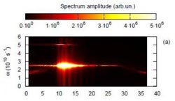
A groundbreaking fabrication technique, based on what is called a DC-augmented capacitively coupled plasma source, affords chip makers unprecedented control of the plasma. This process enables DC-electrode borne electron beams to reach and harden the surface of the mask that is used for printing the microchip circuits. More importantly, the presence of the beam creates a population of suprathermal electrons in the plasma, producing the plasma chemistry that is necessary to protect the mask. The energy of these electrons is greater than simple thermal heating could produce—hence the name “suprathermal.” But how the beam electrons transform themselves into this suprathermal population has been a puzzle.
Now a computer simulation developed at the U.S. Department of Energy's Princeton
Plasma Physics Laboratory in collaboration with the University of Alberta has shed light on this transformation. The simulation reveals that the initial DC-electrode borne beam generates intense plasma waves that move through the plasma like ripples in water. And it is this beam-plasma instability that leads to the generation of the crucial suprathermal electrons.
Understanding the role these instabilities play provides a first step toward still-greater control of the plasma-surface interactions, and toward further increasing the number of transistors on integrated circuits. Insights from both numerical simulations and experiments related to beam-plasma instabilities thus portend the development of new plasma sources and the increasingly advanced chips that they fabricate.
Research Contacts:
I.D. Kaganovich: (609) 243-3277 (ikaganov@pppl.gov)
D. Sydorenko (University of Alberta, Edmonton, Canada)
Abstracts:
TO6.00005 Collisionless acceleration of plasma electrons by intense electron beam
Session: Low Temperature Plasma Science, Engineering and Technology
9:30 AM–11:06 AM, Thursday, November 14, 2013
Media Contact
More Information:
http://www.aps.orgAll latest news from the category: Physics and Astronomy
This area deals with the fundamental laws and building blocks of nature and how they interact, the properties and the behavior of matter, and research into space and time and their structures.
innovations-report provides in-depth reports and articles on subjects such as astrophysics, laser technologies, nuclear, quantum, particle and solid-state physics, nanotechnologies, planetary research and findings (Mars, Venus) and developments related to the Hubble Telescope.


Newest articles

High-energy-density aqueous battery based on halogen multi-electron transfer
Traditional non-aqueous lithium-ion batteries have a high energy density, but their safety is compromised due to the flammable organic electrolytes they utilize. Aqueous batteries use water as the solvent for…

First-ever combined heart pump and pig kidney transplant
…gives new hope to patient with terminal illness. Surgeons at NYU Langone Health performed the first-ever combined mechanical heart pump and gene-edited pig kidney transplant surgery in a 54-year-old woman…

Biophysics: Testing how well biomarkers work
LMU researchers have developed a method to determine how reliably target proteins can be labeled using super-resolution fluorescence microscopy. Modern microscopy techniques make it possible to examine the inner workings…

