World's First Large(Wafer)-Scale Production of III-V Semiconductor Nanowire
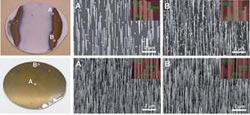
Optical and SEM images of the InAsyP1-y nanowire array. Copyright : UNIST<br>
The research team demonstrated a novel method to epitaxially synthesize structurally and compositionally homogeneous and spatially uniform ternary InAsyP1-y nanowire on Si at wafer-scale using metal-organic chemical vapor deposition (MOCVD). The high quality of the nanowires is reflected in the remarkably narrow PL and X-ray peak width and extremely low ideality factor in the InAsyP1-y nanowire/Si diode.
A nanowire is a nanostructure with a diameter of the order of a nanometer (10-9 meters). Alternatively, nanowires can be defined as structures that have a thickness or diameter constrained to tens of nanometers or less and an unconstrained length. Technology related to nanowires has been selected as one of the 10 Breakthrough Technologies of 2004 by MIT Technology Review.
High-aspect-ratio semiconductors have led to significant breakthroughs in conventional electrical, optical, and energy harvesting devices. Among such structures, III-V semiconductor nanowires offer unique properties arising from their high electron mobility and absorption coefficients, as well as their direct bandgaps.
A common technique for creating a nanowire is Vapor-Liquid-Solid (VLS) synthesis. This process can produce crystalline nanowires of some semiconductor materials. However, metal catalysts, usually expensive noble metals, should be used for initiating the VLS mechanism. In addition, these metal catalysts are known to significantly degrade the quality of semiconductor nanowires by creating deep levels, thus limiting practical applications of nanowires into opto-electronic devices.
In this work, however, Prof. Choi's group developed a novel technique of growing III-V semiconductor nanowires without metal catalysts or nano-patterning. Metal-organic chemical vapor deposition (MOCVD, AIXTRON A200) was used for the growth of the InAsyP1-y. 2 inch Si (111) wafer was cleaned with buffer oxide etch for 1 minute and deionized (DI) water for 2 seconds. Then, the wafer was immediately dipped in poly-L-lysine solution (Sigma-Aldrich inc.) for 3 minutes then rinsed in DI water for 10 seconds. The Si substrate was then loaded into the MOCVD reactor without any delay. The reactor pressure was lowered to 50 mbar with 15liter/min of hydrogen gas flow. Then the reactor was heated to growth temperatures (570 – 630°C), and stabilized for 10 minutes.
Kyoung Jin Choi, Associate Professor at Ulsan National Institute of Science and Technology (UNIST), Korea, and Xiuling Li, Professor at University of Illinois, U.S.A. led the research and this description of the new research was published on the web on May 7 in ACS Nano. (Title: Wafer-Scale Production of Uniform InAsyP1-y Nanowire Array on Silicon for Heterogeneous Integration).
“If we develop new technology which manages the density of nanowire and bandgap energy with further study, it is also possible to produce high-efficiency & low-cost large scale solar cells,” said Prof. Choi. “This technology will give us a chance to lead the research on the new renewable energy.”
Journal information
ACS Nano
Funding information
This work was supported by the Future-based Technology Development Program (Nano Fields) through the National Research Foundation of Korea (NRF) funded by the Ministry of Education, Science and Technology.
Media Contact
All latest news from the category: Power and Electrical Engineering
This topic covers issues related to energy generation, conversion, transportation and consumption and how the industry is addressing the challenge of energy efficiency in general.
innovations-report provides in-depth and informative reports and articles on subjects ranging from wind energy, fuel cell technology, solar energy, geothermal energy, petroleum, gas, nuclear engineering, alternative energy and energy efficiency to fusion, hydrogen and superconductor technologies.


Newest articles

A universal framework for spatial biology
SpatialData is a freely accessible tool to unify and integrate data from different omics technologies accounting for spatial information, which can provide holistic insights into health and disease. Biological processes…

How complex biological processes arise
A $20 million grant from the U.S. National Science Foundation (NSF) will support the establishment and operation of the National Synthesis Center for Emergence in the Molecular and Cellular Sciences (NCEMS) at…

Airborne single-photon lidar system achieves high-resolution 3D imaging
Compact, low-power system opens doors for photon-efficient drone and satellite-based environmental monitoring and mapping. Researchers have developed a compact and lightweight single-photon airborne lidar system that can acquire high-resolution 3D…

