State-of-the-art operating controls with elastic circuits
Elastic circuits Copyright: INM
In future, it will therefore be possible to put console elements or touch sensitive displays on the ergonomically shaped handles of small electrical appliances and household appliances or console elements. Gestures such as lightly touching or wiping the surface still function reliably although the surface is not planar. As a result, in future, conventional buttons, keys or switches will not be necessary.
The developers will be demonstrating their results and the possibilities they offer at stand B46 in hall 2 at this year's Hannover Messe as part of the leading trade fair for R & D and Technology Transfer which takes place from 25th to 29th April.
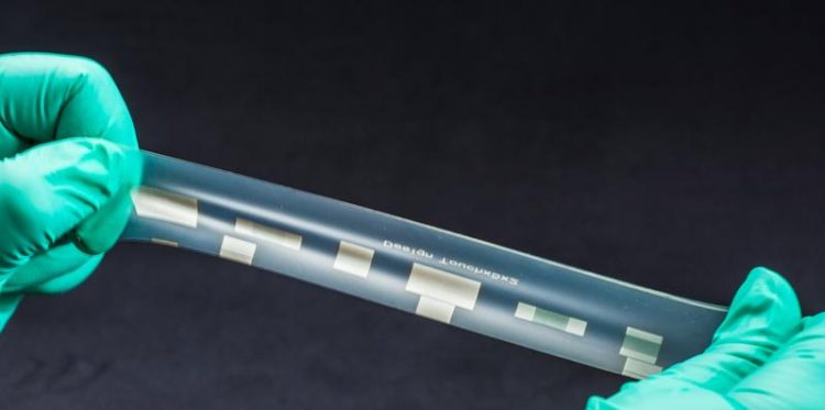
The researchers have now achieved the possibility of such electronic switching on elastic material on silicone foil using a process known as photochemical metallization. In this process, colorless silver compounds are transformed into electrically conductive silver when a photoactive layer is irradiated by UV light.
Peter William de Oliveira, Head of INM’s program division Optical Materials explains, “First, the silicone foils are coated with a photoactive layer of metal oxide nanoparticles. After that, we apply a specially developed fluid containing colorless silver ions”. When this sequence of layers is irradiated with UV light, the silver compound disintegrates on the photoactive layer and the silver ions are reduced to form metallic, electrically conductive silver.
By the use of adjustable pattern, the UV irradiation can be controlled. So, paths or other structures on the carrier material are reduced to form silver. In this way, very narrow conductor paths with widths down to only a few micrometers can be produced on the silicone foil. The electronic circuitry is then transparent to the observer.
Until now, researchers have been able to apply this combination of materials in laboratory format in postcard size. In future, developers would like to extend this manufacturing principle in cooperation with interested partners from industry into a roll-to-roll process. This would make allow a fast, economical and environmentally-friendly manufacturing also in large dimensions including in large formats.
Your contact at the stand B46 in hall 2:
Dr. Michael Opsölder
Jana Staudt
Your expert at INM:
Dr. Peter William de Oliveira
INM – Leibniz Institute for New Materials
Head Optical Materials
Head InnovationCenter INM
Phone: +49681-9300-148
OptiMat@leibniz-inm.de
INM conducts research and development to create new materials – for today, tomorrow and beyond. Chemists, physicists, biologists, materials scientists and engineers team up to focus on these essential questions: Which material properties are new, how can they be investigated and how can they be tailored for industrial applications in the future? Four research thrusts determine the current developments at INM: New materials for energy application, new concepts for medical surfaces, new surface materials for tribological systems and nano safety and nano bio. Research at INM is performed in three fields: Nanocomposite Technology, Interface Materials, and Bio Interfaces.
INM – Leibniz Institute for New Materials, situated in Saarbrücken, is an internationally leading centre for materials research. It is an institute of the Leibniz Association and has about 220 employees.
Media Contact
All latest news from the category: Trade Fair News


Newest articles

A universal framework for spatial biology
SpatialData is a freely accessible tool to unify and integrate data from different omics technologies accounting for spatial information, which can provide holistic insights into health and disease. Biological processes…

How complex biological processes arise
A $20 million grant from the U.S. National Science Foundation (NSF) will support the establishment and operation of the National Synthesis Center for Emergence in the Molecular and Cellular Sciences (NCEMS) at…

Airborne single-photon lidar system achieves high-resolution 3D imaging
Compact, low-power system opens doors for photon-efficient drone and satellite-based environmental monitoring and mapping. Researchers have developed a compact and lightweight single-photon airborne lidar system that can acquire high-resolution 3D…

