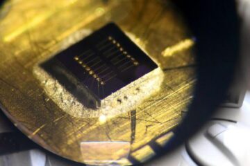
Inexpensive method to create a smooth Silicon Carbide-surface on Silicon-wafers
Silicon Carbide is e.g. used as a substrate for the epitaxial growth of e.g. Gallium Nitride which is used for light-emitting diodes and blue laser. Silicon Carbide wafers, however, are much more expensive than silicon wafers; and silicon carbide surfaces that have been grown on cheap silicon wafers usually show a huge warpage. The invention describes an inexpensive way to create a smooth and high-quality silicon carbide surface on silicon-wafers with state-of-the-art CMOS compatible process.
Further Information: PDF
Bayerische Patentallianz GmbH
Phone: +49 89 5480177-0
Contact
Peer Biskup
Media Contact
All latest news from the category: Technology Offerings
Newest articles

Sea slugs inspire highly stretchable biomedical sensor
USC Viterbi School of Engineering researcher Hangbo Zhao presents findings on highly stretchable and customizable microneedles for application in fields including neuroscience, tissue engineering, and wearable bioelectronics. The revolution in…

Twisting and binding matter waves with photons in a cavity
Precisely measuring the energy states of individual atoms has been a historical challenge for physicists due to atomic recoil. When an atom interacts with a photon, the atom “recoils” in…
Nanotubes, nanoparticles, and antibodies detect tiny amounts of fentanyl
New sensor is six orders of magnitude more sensitive than the next best thing. A research team at Pitt led by Alexander Star, a chemistry professor in the Kenneth P. Dietrich…

