Shrinking of Barrier Films into Nanotechnology Geometries
Milestone to Fulfill Metallization Requirements for Chip Manufacturing into Next Decade
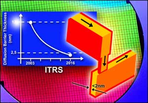
Infineon Technologies (FSE/NYSE: IFX) today announced that its Munich Research Labs have demonstrated, by shrinking present film thicknesses into nanotechnology geometries, that the stringent requirements of thin encapsulation films in metallization schemes of future chip generations will be met. The results shows that thin barrier films, key components for advanced copper chip wiring, will meet the electrical and functional demands defined for the end of the International Roadmap for Semiconductors (ITRS), which extends to 2016. The ITRS expects a reduction of the barrier thickness from 12nm (100nm node, 2003) to 2.5 nm (22 nm node, 2016). The goal of the Infineon researchers was to investigate the scaling limits of the current Ta /TaN barrier technology and its compatibility with the end-of-roadmap target values.
The Infineon researchers have successfully performed an electrical assessment of the integration of ultrathin metallic barrier films encapsulating copper metal lines in advanced chip metallization systems. These electrically conducting films separate the copper metal lines from the surrounding dielectrics used for electrical isolation. Hermetic encapsulation of copper lines has to prevent copper diffusion into the dielectric isolation, and in particular from reaching the transistors below the wiring layers in the chip, as at transistor level copper is readily destroying device operation.
To achieve best chip performance, these barrier films have to be processed as thin as possible for two reasons: Ultrathin barrier films around copper wires leave a maximum of space for the highly conducting copper wire. Furthermore, in the vertical interconnects between the layers of copper wires (via holes) the current flow crosses the barrier film. An ultrathin film provides a very low electrical resistance.
The obtained results demonstrated barrier functionality against copper diffusion with film thicknesses of less than 2 nanometers, meeting the same stringent reliability requirements as 50nm thick barrier films in a current semiconductor product. The electrical resistance of via holes with such thin barrier films is sufficiently low to realize such structures in high-speed microprocessor chips expected to come to production by the middle of next decade.
“ With its lower electrical resistance and its higher ruggedness against electro-migration copper shows clear advantages for high performance ICs. But to make this material usable as an interconnect material for future chip generations, great effort has to be spent on preventing any diffusion of copper,“ said Prof. Dr. Karl Joachim Ebeling, head of corporate research at Infineon Technologies. “The recent results mark a significant milestone to provide all the high sophisticated technologies needed to manufacture the further shrinked next chip generations.”
The manufacturing tools needed for the fabrication of chip generations in the timeframe beyond 2010 do not yet exist. Infineon overcame this issue by extending the unit processes in existing manufacturing tools far beyond the requirements in today’s products. This allows the reliable deposition of thin contiguous functional films with sub-2nm thicknesses as required in the metallization schemes for the generation of microprocessors which is expected to be in production not earlier than in 2016. The results therefore also demonstrate that the use of state-of-the-art thin film deposition techniques may be extended for future chip generations rather than requiring novel atomic layer deposition techniques.
The copper wires were fabricated with the damascene metallization technique. In this technique, grooves and holes are filled by deposition of metal followed by a complete removal of all metal covering the filled structures by chemical mechanical polishing. The technique is named after the way ornaments were once accomplished in damascene swords. The silicon wafers used for the electrical assessment of the embedded copper lines were processed with standard semiconductor manufacturing equipment and processes developed in Infineon´s Munich cleanrooms.
The results from Infineon’s Corporate Research demonstrate that thin barrier films will meet the requirements regarding electrical properties and functionality through the end of the ITRS in 2016. The ITRS describes the technological and material demands of future chip generations. Regarding the barrier films for the wiring schemes in end-of-roadmap chip generations the latest edition of the roadmap noted: “no manufacturable solution”. Infineon has demonstrated now, that this very thin barrier films are manufacturable, and it is expected that the next edition of the ITRS will be updated accordingly.
Media Contact
More Information:
http://www.infineon.comAll latest news from the category: Information Technology
Here you can find a summary of innovations in the fields of information and data processing and up-to-date developments on IT equipment and hardware.
This area covers topics such as IT services, IT architectures, IT management and telecommunications.


Newest articles

High-energy-density aqueous battery based on halogen multi-electron transfer
Traditional non-aqueous lithium-ion batteries have a high energy density, but their safety is compromised due to the flammable organic electrolytes they utilize. Aqueous batteries use water as the solvent for…

First-ever combined heart pump and pig kidney transplant
…gives new hope to patient with terminal illness. Surgeons at NYU Langone Health performed the first-ever combined mechanical heart pump and gene-edited pig kidney transplant surgery in a 54-year-old woman…

Biophysics: Testing how well biomarkers work
LMU researchers have developed a method to determine how reliably target proteins can be labeled using super-resolution fluorescence microscopy. Modern microscopy techniques make it possible to examine the inner workings…

