Highly Conductive Germanium Nanowires Made by a Simple, One-Step Process
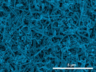
Image courtesy of Jay Switzer Scanning electron micrograph image of germanium nanowires electrodeposited onto an indium tin oxide electrode from aqueous solution.
The Science
For the first time, germanium nanowires have been deposited on indium tin oxide substrate by a simple, one-step process called electrodeposition.
The Impact
The germanium nanowires produced by this method have superior electronic properties compared to silicon and can be used as high-capacity anode material for lithium-ion batteries, but the nanowires were previously too expensive and difficult to produce. This process may resolve the cost issue to advance this battery technology.
Summary
Germanium is a semiconductor that has superior electronic properties compared to silicon, and is being considered as a replacement for silicon in semiconductor technology. It is also an attractive anode material for lithium-ion batteries because it has a large theoretical charge-discharge capacity compared to graphite and high lithium ion diffusivity at room temperature compared to silicon.
The large volume changes associated with charge-discharge processes require anodes be made of high-surface-area nanostructures of germanium. A lack of inexpensive and simple methods to produce germanium nanostructures has so far limited their use in battery electrode applications.
Now, researchers at the Missouri University of Science and Technology have shown for the first time that germanium nanowires can be deposited by a simple, one-step process called electrodeposition that could provide a low cost route to fabricate these anodes.
The nanowires were grown on an indium tin oxide substrate. An electrochemical reduction produces tiny indium nanoparticles on the indium tin oxide surface, which act as sites for the nucleation and crystallization of germanium nanowires.
The nanowire diameter can be controlled by the solution temperature: wires grown at room temperature have an average diameter of 35 nanometers, whereas those grown at 95°C have an average diameter of 100 nanometers. The germanium nanowires produced by this method are highly conductive, because they contain a small amount of indium impurity (~0.2 atomic percent), making them ideal for lithium-ion battery applications.
Funding
DOE Office of Science, Basic Energy Sciences.
Publication
N.K. Mahenderkar, Y.C. Liu, J. A. Koza, J.A. Switzer, “Electrodeposited germanium nanowires.” ACS Nano 9, 9524–9530 (2014). [DOI: 10.1021/nn503784d]
Contact Information
Kristin Manke
kristin.manke@science.doe.gov
Media Contact
All latest news from the category: Materials Sciences
Materials management deals with the research, development, manufacturing and processing of raw and industrial materials. Key aspects here are biological and medical issues, which play an increasingly important role in this field.
innovations-report offers in-depth articles related to the development and application of materials and the structure and properties of new materials.


Newest articles

A universal framework for spatial biology
SpatialData is a freely accessible tool to unify and integrate data from different omics technologies accounting for spatial information, which can provide holistic insights into health and disease. Biological processes…

How complex biological processes arise
A $20 million grant from the U.S. National Science Foundation (NSF) will support the establishment and operation of the National Synthesis Center for Emergence in the Molecular and Cellular Sciences (NCEMS) at…

Airborne single-photon lidar system achieves high-resolution 3D imaging
Compact, low-power system opens doors for photon-efficient drone and satellite-based environmental monitoring and mapping. Researchers have developed a compact and lightweight single-photon airborne lidar system that can acquire high-resolution 3D…

