Unique X-ray Topography Based Defect Characterization for SiC Wafers
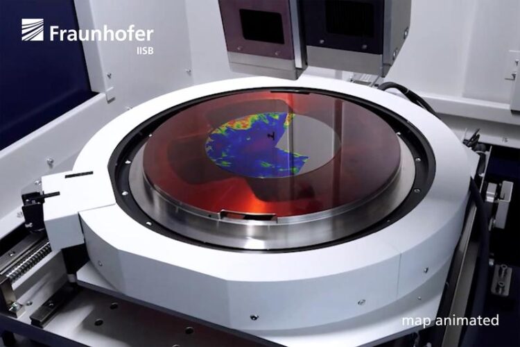
In-tool view of the Rigaku XRTmicron with animated defect map to showcase the non-destructive, high-speed metrology process across the entire wafer surface
(c) Elisabeth Iglhaut / Fraunhofer IISB
Honored with Georg Waeber Innovation Award 2023.
A team from Rigaku SE and Fraunhofer IISB has established a new semiconductor material characterization method. They succeeded in developing an industry-ready X-ray topography system and in employing defect detection and quantification algorithms, achieving a unique material characterization method for silicon carbide (SiC) wafers. SiC is an excellent semiconductor for application areas like electric mobility, energy supply, industrial infrastructure up to sensors and quantum technologies. Now, Dr. Kranert and Dr. Reimann from Fraunhofer IISB and Dr. Hippler, Managing Director Rigaku Europe SE, have won the Georg Waeber Innovation Award 2023 from the Förderkreis für die Mikroelektronik e.V.
Pioneering holistic material defect characterization with X-ray topography
In 2021, Rigaku SE and Fraunhofer IISB have founded the Center of Expertise for X-ray Topography, a joint lab that is located at the IISB’s headquarters in Erlangen, Germany. Here, the cross-organizational team has now developed a new metrology that is non-destructive, robust, reliable, high-throughput and therefore capable of swiftly detecting all relevant crystallographic defects in SiC substrates. For the first time worldwirde, this innovation realized the holistic approach of setting up the measurement device, i.e., the X-ray topography (XRT) tool as well as formulating appropriate measurement and analysis routines that specifically meet the industry’s demands for speed, reliability, and accuracy. The development process was supported by rigorous scientific validation of the results, a crucial factor for the acceptance of a new approach in the industry.

Dr. Michael Hippler, Managing Director of Rigaku Europe SE, Dr. Christian Reimann and Dr. Christian Kranert from Fraunhofer IISB with their award certificate in front of the Rigaku XRTmicron tool at the Center of Expertise for X-ray Topography at the IISB. (c) Elisabeth Iglhaut / Fraunhofer IISB
Until now, no such industry-ready metrology existed for the early stages of SiC power electronics manufacturing, especially at substrate or crystal (commonly referred to as the “puck”) level. This breakthrough in SiC substrate inspection makes it no longer necessary to, e.g., destructively defect etch and discard semiconductor substrates for characterization, as is currently often the case. In consequence, the developed XRT metrology is superior to these existing substrate characterization methods employed in the industry, ultimately leading to substantial cost savings.
Effectively, this technology, developed in Germany, provides everything needed to become the industry standard for specifying and controlling substrate quality in production as well as for R&D substrate and device manufacturers worldwide. The success of this joint innovation is vividly illustrated by the new business, which Rigaku has successfully established in less than two years. Now, the Japan-based company is the world’s leading supplier of XRT tools for SiC substrate and device manufacturing.
The innovative metrology approach has been driven significantly by Dr. Michael Hippler, Managing Director of Rigaku Europe SE, and Dr. Christian Kranert with Dr. Christian Reimann, both group managers in the Fraunhofer IISB’s Materials department. Hence the scientists were selected for the Georg Waeber Innovation Award 2023 by the Förderkreis für die Mikroelektronik e.V. (Microelectronics Promotion Society). The Förderkreis is an association of industry companies, two Fraunhofer institutes, four chairs of the University of Erlangen-Nuremberg and the Nuremberg Chamber of Commerce and Industry. The main objective is to foster a smooth exchange between science and industry, which is manifested in the Georg Waeber Innovation Award. The award is presented annually for outstanding scientific achievements and places a strong emphasis on the advancement of knowledge in microelectronics and its practical application in the industry. On October 25, 2023, Dr. Hippler, Dr. Reimann and Dr. Kranert received the award during a ceremony at Fraunhofer IISB in Erlangen.
Paving the way for the next generation of SiC power electronics
SiC semiconductor devices play a pivotal role in the power electronics industry. As a replacement for conventional silicon-based power electronics, SiC has the potential to enhance energy efficiency while reducing system costs. It is relevant across various application areas from electric mobility and transportation, sustainable energy supply, industrial infrastructure up to sensors and quantum technologies even under harsh operating conditions. Consequently, processing low-cost, energy-efficient, and highly reliable SiC power devices is a critical endeavor with the worldwide electrification trend. The production capacities for SiC wafers experience significant growth, which goes hand in hand with an increasing demand for wafer inspection and metrology within the SiC industry. In particular, manufacturers of substrates and power devices require precice information regarding the quality of substrates in terms of crystallographic defects, their distribution across the entire wafer area, and absolute quantities.
Infolinks
Detailed technical information on XRT and the Center of Expertise for X-ray Topography:
www.iisb.fraunhofer.de/xrt
Förderkreis für die Mikroelektronik e.V. (Microelectronics Promotion Society):
www.foerderkreis-mikroelektronik.org
Rigaku SE
Founded in Japan in 1951, Rigaku has maintained its position at the forefront of analytical and industrial instrumentation technology. Rigaku and its subsidiaries form a global group dedicated to the fields of general analytical instrumentation and life sciences. Recognised as a world leader in X-ray Spectrometry, Diffraction, Optics, Small Molecule and Protein Crystallography and Semiconductor Metrology, Rigaku currently employs over 1,800 professionals dedicated to the manufacture and support of its analytical instruments. These instruments are used in over 90 countries to ad-vance research, development, and quality assurance. On a global scale, Rigaku con-sistently promotes partnerships, dialogue, and innovation within the scientific and industrial communities.
Fraunhofer IISB
The Fraunhofer IISB in Erlangen, Germany, specializes in wide-bandgap semiconduc-tors and efficient power electronics. Here, device know-how merges with complex system development, especially for e-mobility and sustainable energy supply.
The institute bundles its activities in the two business units Power Electronic Systems and Semiconductors. In doing so, it comprehensively covers the entire value chain from basic materials, through semiconductor devices, processes, and module tech-nologies, to complete electronics and energy systems. As a unique center of excel-lence in Europe for the semiconductor material silicon carbide (SiC), the IISB is a pioneer in the development of highly efficient power electronics, even for extreme requirements.
Diese Pressemitteilung ist als Kurzversion auch auf Deutsch verfügbar:
www.iisb.fraunhofer.de/presse.
The press releases of Fraunhofer IISB are accessible online at: www.iisb.fraunhofer.de/press
There you will also find photo material for editorial use.
Wissenschaftliche Ansprechpartner:
Dr. Christian Reimann
Group Manager Silicon and Special Materials
Fraunhofer IISB
Schottkystrasse 10, 91058 Erlangen, Germany
Phone +49 9131 761 272
christian.reimann@iisb.fraunhofer.de
https://www.iisb.fraunhofer.de
Weitere Informationen:
https://www.iisb.fraunhofer.de/ Fraunhofer IISB Homepage
https://www.linkedin.com/company/fraunhofer-iisb/ Fraunhofer IISB on LinkedIn
https://www.iisb.fraunhofer.de/en/research_areas/materials/x-ray-topography.html Center of Expertise for X-ray Topography
https://www.rigaku.com/ Rigaku SE Homepage
https://foerderkreis-mikroelektronik.org/ Förderkreis für die Mikroelektronik e.V. (Microelectronics Promotion Society)
Media Contact
All latest news from the category: Process Engineering
This special field revolves around processes for modifying material properties (milling, cooling), composition (filtration, distillation) and type (oxidation, hydration).
Valuable information is available on a broad range of technologies including material separation, laser processes, measuring techniques and robot engineering in addition to testing methods and coating and materials analysis processes.


Newest articles

Faster, more energy-efficient way to manufacture an industrially important chemical
Zirconium combined with silicon nitride enhances the conversion of propane — present in natural gas — needed to create in-demand plastic, polypropylene. Polypropylene is a common type of plastic found…

Energy planning in Ghana as a role model for the world
Improving the resilience of energy systems in the Global South. What criteria should we use to better plan for resilient energy systems? How do socio-economic, technical and climate change related…

Artificial blood vessels could improve heart bypass outcomes
Artificial blood vessels could improve heart bypass outcomes. 3D-printed blood vessels, which closely mimic the properties of human veins, could transform the treatment of cardiovascular diseases. Strong, flexible, gel-like tubes…

