Tiny wires, maximum power

Groundbreaking interconnection technology using 200 nm nanowires to realize tomorrow’s high-performance electronics.
(c) Fraunhofer IZM
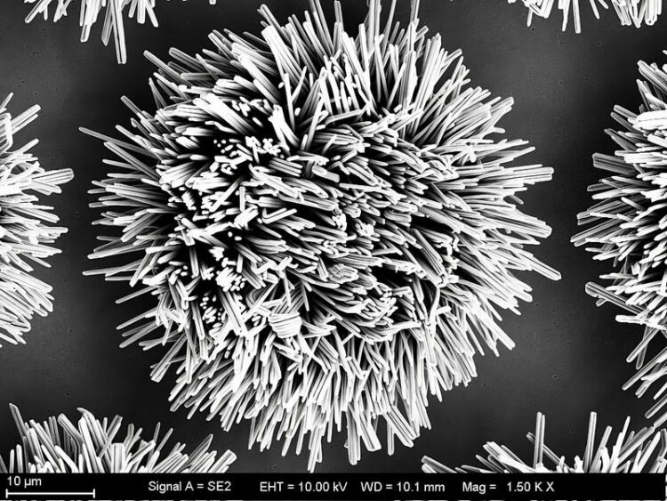
Nanowire contacts push the boundaries for high-performance electronics.
Space comes at a premium on electronic chips: Powerful electronics need more and more connections, crammed into smaller and smaller spaces. Established technologies are reaching the limits of what is physically possible. Now, researchers at Fraunhofer IZM-ASSID have teamed up with other partners to level up a connection technology patented by NanoWired GmbH that uses wires at a nanometer scale. The team demonstrated how the novel technology could be used in the industrial production of 300 mm wafers.
To guarantee efficiency and technological sovereignty in our digital future, the world needs high-performance supercomputers. In high-performance computing, data centers need to handle unimaginable amounts of data and conduct extremely complex calculations. This is essential whenever complicated operations need to be processed at high speed, such as scientific simulations or algorithms. Supercomputers are already being used to optimize traffic flows, logistics, industrial operations, and high-precision medical tasks. And high-performance computing is just one of the many applications that will need powerful, efficient, and reliable computing technology.
Meeting these challenging demands needs new interconnection technologies. The basic idea is simple: The smaller the pitch, i.e. the space between electronic contacts, the more transistors and electronic circuits can be fitted on a chip and the more powerful the chip becomes. The old standard for flip-chip designs was to use copper bumps for soldering, but this technology is coming up against its physical limitations when the devices are shrunk more and more, as the solder can leak and cause short circuits in the system.

close-up (c) Fraunhofer IZM
Looking for innovative alternatives, junior professor Dr. Iuliana Panchenko and her team at Fraunhofer IZM-ASSID decided to try new interconnection techniques for contacts shrunk down to less than 10 micrometers. As part of the Fraunhofer-funded SME project “NanoInt”, they and their partners in industry and academia thought up a promising option that relies on copper nanowires and evaluated it successfully for use on 300mm silicon wafers.
Compared to other options like copper soldering or solder bumps or hybrid and compression bonding, using a direct connection in the form of copper nanowires offers several advantages. The pluggable solution (nanowire to nanowire) means that designs with different heights can be realized. No other metal materials need to be used, the resulting system is mechanically robust, and it gives chip designers lots of freedom. The connections can be made at room temperature and with only limited bonding pressure, which makes the technology easy on resources and suitable for thin or heat-sensitive chips.
During the first part of the project, the researchers focused on ways to grow the nanowires as evenly as possible at the contact points spread out across the entire 300 mm wafer. They managed to do so by using special membranes with tiny pores. These pores determine how thick the nanowire would become, and they can be varied for thicknesses from 100 nm to 1 µm. Finding the right pore diameter is crucial to establish a reliable and properly conductive connection. Once the membrane is in place, a galvanic process is started, and the copper nanowires can grow through the pores, with the lengths of the nanowires varying by approx. 20 percent as a result of tweaks to the process. The project team also developed the right process flow to protect the nanowires during etching, which is necessary to remove the conductive copper seeding layer from the wafer.
The novel connection technology had to be evaluated for its practical feasibility, so the researchers tested how the process could be integrated in an industrial process chain. They defined the optimum parameters for assembling the systems and applied them in testing with particular attention to the technology’s reproducibility, homogeneity, mechanical robustness, and feasibility for industrial use.
To mark the end of the project, the project partners produced a 300 mm silicon wafer with homogeneous nanowire bumps and nanowire connections in a chip-to-chip layout, showing how the technology could be integrated in 2.5D to 3D system designs without need for additional fluxing agents. The technology is already being rolled out into industrial use, and additional research projects are planned to shrink the contacts down to 10 or even 5 micrometers. In future, new applications for nanowires are possible for complex packages that use fine-pitch or larger contact areas.
The partners on the “NanoInt” project included NanoWired GmbH, Fraunhofer IMWS, and the IAVT at the Technical University of Dresden.
(Text: Olga Putsykina)
Wissenschaftliche Ansprechpartner:
Jun.-Prof. Dr.-Ing. Iuliana Panchenko l Phone +49 351 795572-814l iuliana.panchenko@assid.izm.fraunhofer.de | Fraunhofer Institute for Reliability and Microintegration IZM-ASSID I Ringstr. 12 I 01468 Moritzburg | www.izm.fraunhofer.de |
Originalpublikation:
https://www.izm.fraunhofer.de/en/news_events/tech_news/tiny-wires-maximum-power….
Media Contact
All latest news from the category: Power and Electrical Engineering
This topic covers issues related to energy generation, conversion, transportation and consumption and how the industry is addressing the challenge of energy efficiency in general.
innovations-report provides in-depth and informative reports and articles on subjects ranging from wind energy, fuel cell technology, solar energy, geothermal energy, petroleum, gas, nuclear engineering, alternative energy and energy efficiency to fusion, hydrogen and superconductor technologies.
Newest articles
Faster, more energy-efficient way to manufacture an industrially important chemical
Zirconium combined with silicon nitride enhances the conversion of propane — present in natural gas — needed to create in-demand plastic, polypropylene. Polypropylene is a common type of plastic found…

Energy planning in Ghana as a role model for the world
Improving the resilience of energy systems in the Global South. What criteria should we use to better plan for resilient energy systems? How do socio-economic, technical and climate change related…

Artificial blood vessels could improve heart bypass outcomes
Artificial blood vessels could improve heart bypass outcomes. 3D-printed blood vessels, which closely mimic the properties of human veins, could transform the treatment of cardiovascular diseases. Strong, flexible, gel-like tubes…


