High-performance ion implantation

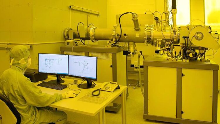
Operator terminal and beamline of the new ion implanter - a crucial tool for innovative semiconductor devices
FBH/P. Immerz
– the basis for innovative semiconductor devices.
The Berlin-based Ferdinand-Braun-Institut (FBH) recently put a sophisticated ion implanter system from High Voltage Engineering Europa B.V. into operation. The highly versatile tool extends the technological capabilities of FBH for in-house research and customer processes. With three different ion sources and the ability to heat substrates, the implanter is ideally suited for the development of innovative semiconductor devices.
Among other things, the system enables doping implantations of wide-bandgap semiconductors, whose outstanding material properties are to be used in future power electronics applications.
Ion implantation is one of the key processes in manufacturing microelectronic devices, which is used to introduce foreign atoms into semiconductor layers. In this process, charged particles (ions) are shot at semiconductor materials and thus introduced (implanted) into a material layer. With this key technology of the semiconductor industry, material properties can be modified in a targeted manner.
Flexible system for compound semiconductors and special substrates
The novel ion implanter offers high implantation currents of up to 2 mA and covers acceleration voltages from 5 keV to 500 keV. This allows materials to be systematically modified even at high implantation doses within industry-compatible process times. A sputtering source can also be used to implant materials with very high melting points, such as the special metals tungsten, molybdenum, tantalum, and niobium. This opens up further technological possibilities. In addition to a gas source, the system is equipped with two furnaces to implant low melting metals.
The new implanter offers another special feature: with a special sample holder, substrates can be heated up to 500 °C. This enables activation of the dopants during implantation, for example in wide-gap semiconductors. The possibilities for selective isolation and doping make the new ion implanter an important technical foundation at FBH for the development of innovative planar integration processes in materials like gallium nitride, aluminum nitride, and gallium oxide.
The procurement of the ion implanter and the required installation work in the cleanroom was funded by the Federal Ministry of Education and Research (BMBF) within the framework of “Research Fab Microelectronics Germany (FMD)” (funding reference 16FMD02).
Media Contact
All latest news from the category: Power and Electrical Engineering
This topic covers issues related to energy generation, conversion, transportation and consumption and how the industry is addressing the challenge of energy efficiency in general.
innovations-report provides in-depth and informative reports and articles on subjects ranging from wind energy, fuel cell technology, solar energy, geothermal energy, petroleum, gas, nuclear engineering, alternative energy and energy efficiency to fusion, hydrogen and superconductor technologies.
Newest articles
Faster, more energy-efficient way to manufacture an industrially important chemical
Zirconium combined with silicon nitride enhances the conversion of propane — present in natural gas — needed to create in-demand plastic, polypropylene. Polypropylene is a common type of plastic found…

Energy planning in Ghana as a role model for the world
Improving the resilience of energy systems in the Global South. What criteria should we use to better plan for resilient energy systems? How do socio-economic, technical and climate change related…

Artificial blood vessels could improve heart bypass outcomes
Artificial blood vessels could improve heart bypass outcomes. 3D-printed blood vessels, which closely mimic the properties of human veins, could transform the treatment of cardiovascular diseases. Strong, flexible, gel-like tubes…


