Silicon-graphene hybrid plasmonic waveguide photodetectors beyond 1.55 μm
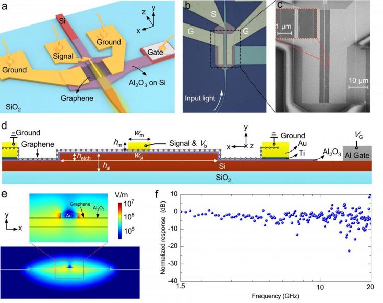
a. Schematic configuration; b. Optical microscope; c. SEM pictures; d. Cross-section of the present silicon-graphene hybrid plasmonic waveguide with the signal electrode at the middle and the ground electrodes at both sides (here the metal-graphene-metal sandwich structure is utilized); e. The electric field component distribution of the quasi-TE0 mode for the optimized silicon-graphene hybrid plasmonic waveguide; f. Measured frequency response of Device B operating at ¦Ë=2μm (bias voltage: -0.5 V, gate voltage: 2.9 V). Credit: Jingshu Guo, Jiang Li, Chaoyue Liu, Yanlong Yin, Wenhui Wang, Zhenhua Ni, Zhilei Fu, Hui Yu, Yang Xu, Yaocheng Shi, Yungui Ma, Shiming Gao, Liming Tong and Daoxin Dai
However, the realization of high-performance silicon-based waveguide photodetectors beyond 1.55 μm still faces challenges since there are some fabrication issues as well as wavelength-band limitations.
As an alternative, two-dimensional materials (e.g., graphene) provide a promising solution because of the ability for broad operation wavelength-bands and the advantage of avoiding structure mismatch in the design and fabrication.
In the paper published in Light: Science & Applications, scientists from Zhejiang University and Southeast University in China proposed and demonstrated high-performance waveguide photodetectors beyond 1.55 μm by introducing a novel silicon-graphene hybrid plasmonic waveguide.
In particular, an ultra-thin wide silicon ridge core region with a metal cap atop is introduced to obtain a unique mode field profile, so that light absorption of graphene is enhanced. Furthermore, the fabrication is easy and the graphene-metal contact resistance is reduced, compared to the previous silicon-graphene hybrid waveguides.
For example, the graphene absorption efficiencies are as high as 54.3% and 68.6% for 20 μm-long and 50 μm-long absorption regions, when operating at 1.55 μm and 2 μm, respectively.
For the fabricated photodetectors operating at 2 μm, the measured 3 dB-bandwidths are >20 GHz (limited by the experimental setup), while the responsivities are 30-70 mA/W for 0.28 mW input optical power under -0.3V bias voltage. For the photodetectors operating at 1.55 μm, the 3 dB-bandwidth is >40 GHz (limited by the setup), while the measured responsivity is about 0.4 A/W for 0.16 mW input optical power under -0.3V bias voltage.
In this work, the mechanisms in graphene photodetectors are analyzed carefully, which suggested that the photo-thermoelectric effect is the dominant mechanism for photo-response when operating at zero bias voltage.
When the photodetector operates at non-zero bias voltages, the dominant mechanism becomes the bolometric or photoconductive effect. This comprehensive analysis helps better understand the photocurrent generation in the graphene-metal interfaces.
These scientists summarize the highlights of their work:
“We have proposed and demonstrated high-performance silicon-graphene hybrid plasmonic waveguide photodetectors beyond 1.55 μm. In particular, a novel silicon-graphene hybrid plasmonic waveguide was used by introducing an ultra-thin wide silicon ridge core region with a metal cap atop. The optical modal filed is manipulated in both vertical and horizontal directions.
Thus, the light absorption in graphene is enhanced, meanwhile the metal absorption loss is minimized. This greatly helps achieve sufficient light absorption of graphene within a short absorption region.”
“The silicon-graphene waveguide photodetectors operating at 2 μm were demonstrated with a 3 dB-bandwidth over 20 GHz. The measured responsivity is 30-70 mA/W at the bias voltage of -0.3V for input optical power of 0.28 mW. The photodetector at 1.55 μm was also demonstrated with excellent performances. The present work paves the way for achieving high-responsivity and high-speed waveguide photodetectors on silicon for near/mid-infrared wavelength-bands” they added.
“In future works, more efforts should be given to introduce some special junction structures to minimize the dark current and further extend the operation wavelength-band. Graphene waveguide photodetectors may play an important role in mid-infrared silicon photonics, which will play an important role in time resolved spectroscopy, lab-on-chip sensing, nonlinear photonics, as well as optical communication” they said.
Media Contact
More Information:
http://dx.doi.org/10.1038/s41377-020-0263-6All latest news from the category: Materials Sciences
Materials management deals with the research, development, manufacturing and processing of raw and industrial materials. Key aspects here are biological and medical issues, which play an increasingly important role in this field.
innovations-report offers in-depth articles related to the development and application of materials and the structure and properties of new materials.


Newest articles

A universal framework for spatial biology
SpatialData is a freely accessible tool to unify and integrate data from different omics technologies accounting for spatial information, which can provide holistic insights into health and disease. Biological processes…

How complex biological processes arise
A $20 million grant from the U.S. National Science Foundation (NSF) will support the establishment and operation of the National Synthesis Center for Emergence in the Molecular and Cellular Sciences (NCEMS) at…

Airborne single-photon lidar system achieves high-resolution 3D imaging
Compact, low-power system opens doors for photon-efficient drone and satellite-based environmental monitoring and mapping. Researchers have developed a compact and lightweight single-photon airborne lidar system that can acquire high-resolution 3D…

