New method promises easier nanoscale manufacturing
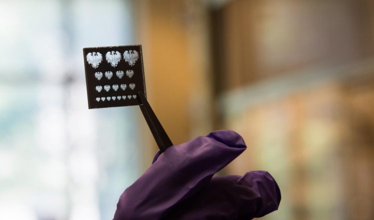
A 'mask' or stencil used to pattern nano materials with a new process that promises to make them far easier to make into LEDs, solar cells, transistors and other electronics. Credit: University of Chicago
The new research, published July 28 in Science, is expected to make such materials easily available for eventual use in everything from LED displays to cellular phones to photodetectors and solar cells. Though nanomaterials are promising for future devices, ways to build them into complex structures have been limited and small-scale.
“This is a step needed to move quantum dots and many other nanomaterials from proof-of-concept experiments to real technology we can use,” said co-author Dmitri Talapin, professor of chemistry at UChicago and a scientist with the Center for Nanoscale Materials at Argonne. “It really expands our horizons.”
The foundation of modern computing is a tiny switch called the transistor, made billions at a time by a technique called photolithography. This process, which has made smartphones cheap and ubiquitous, carves a stencil out of a layer of organic polymer by laying down a patterned “mask” and illuminating it with ultraviolet light.
After the new material is deposited on top, the polymer stencil is lifted off to reveal the pattern. Several rounds of such patterning build a miniature transistor onto the material.
But the method has its limitations. Only a few materials can be patterned this way; it was originally developed for silicon, and as silicon's half-century reign over electronics reaches its end, scientists are looking ahead to the next materials.
One such avenue of interest is nanomaterials–tiny crystals of metals or semiconductors. At this scale, they can have unique and useful properties, but manufacturing devices out of them has been difficult.
The new technique, called DOLFIN, makes different nanomaterials directly into “ink” in a process that bypasses the need to lay down a polymer stencil. Talapin and his team carefully designed chemical coatings for individual particles. These coatings react with light, so if you shine light through a patterned mask, the light will transfer the pattern directly into the layer of nanoparticles below–wiring them into useful devices.
“We found the quality of the patterns was comparable to those made with state-of-the-art techniques,” said lead author Yuanyuan Wang, postdoctoral researcher at UChicago. “It can be used with a wide range of materials, including semiconductors, metals, oxides or magnetic materials–all commonly used in electronics manufacturing.”
###
The team is working towards commercializing the DOLFIN technology in partnership with UChicago's Polsky Center for Entrepreneurship and Innovation.
Citation: Yuanyuang Wang, Igor Fedlin, Hao Zhang, Dmitri V. Talapin, “Direct optical lithography of functional inorganic nanomaterials,” Science. Funding: U.S. Department of Defense, National Science Foundation, U.S. Department of Energy, II-VI Foundation.
Media Contact
All latest news from the category: Materials Sciences
Materials management deals with the research, development, manufacturing and processing of raw and industrial materials. Key aspects here are biological and medical issues, which play an increasingly important role in this field.
innovations-report offers in-depth articles related to the development and application of materials and the structure and properties of new materials.


Newest articles

A universal framework for spatial biology
SpatialData is a freely accessible tool to unify and integrate data from different omics technologies accounting for spatial information, which can provide holistic insights into health and disease. Biological processes…

How complex biological processes arise
A $20 million grant from the U.S. National Science Foundation (NSF) will support the establishment and operation of the National Synthesis Center for Emergence in the Molecular and Cellular Sciences (NCEMS) at…

Airborne single-photon lidar system achieves high-resolution 3D imaging
Compact, low-power system opens doors for photon-efficient drone and satellite-based environmental monitoring and mapping. Researchers have developed a compact and lightweight single-photon airborne lidar system that can acquire high-resolution 3D…

