Customized silicon chips
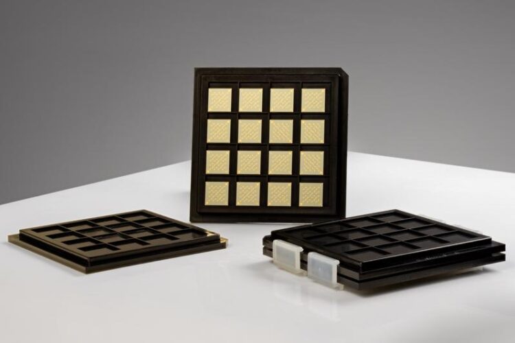
OFET substrates from Fraunhofer IPMS in a waffle pack
(c) Sebastian Lassak / Fraunhofer IPMS
…from Saxony for material characterization of printed electronics.
How efficient are new materials? Does changing the properties lead to better conductivity? The Fraunhofer Institute for Photonic Microsystems IPMS develops and manufactures silicon substrates for this purpose. This enables the fundamental electrical characterization of materials such as a novel graphene emulsion. Customized designs enable the optimal measurement of semiconductors and conductors.

OFET substrates from Fraunhofer IPMS as wafer. (c) Sebastian Lassak / Fraunhofer IPMS
Organic semiconductors are key components in organic electronics and photovoltaics. They are used to make flexible electronic devices and printed solar cells. Typical for this class of materials are low temperature processes as well as large area deposition and patterning using various coating and printing techniques. The active semiconductor materials significantly determine the performance of the entire system.
Therefore, an easy to handle and reliable electronic characterization of conductivity, carrier mobility, contact resistance and on/off current ratio of these semiconductors is an essential requirement for material and process developers.
Fraunhofer IPMS develops and manufactures silicon substrates with single transistor structures in bottom-gate architecture, which are used for the fabrication of organic field-effect transistors (OFETs) or for the characterization of electrical material parameters of conductive materials, e.g. for organic photovoltaics.
Project Manager Thomas Stoppe explains: “Our substrates are already well established in R&D at international research institutions. We now want to focus more on customer-specific solutions and are continuously developing the technology to better meet the needs of our industrial partners. There is a rapidly growing market, especially in the field of organic electronics, and our substrates enable targeted, simple and reproducible measurement of the electrical properties of semiconductors and conductive materials.”
The possibilities for material characterization have been demonstrated with recent results such as the study of a commercial graphene emulsion. These results will be presented at the iCampus-Cottbus Conference iCCC2024 in Cottbus in May 2024 and subsequently published in the Journal of Sensors and Sensor Systems.
Already from April 9 to 12, the developed chips will be presented at the “analytica” trade fair in Munich. Interested users will have the opportunity to talk to experts at the Fraunhofer IPMS stand A3.407. Appointments can be made in advance via the Fraunhofer IPMS website.
Advantages of Fraunhofer IPMS Substrates
The access to the existing microsystem technology of the Fraunhofer IPMS offers significant advantages, such as the high-precision and reproducible fabrication of the chips and the flexible adaptation of the technology to the individual requirements of the target application. This enables different material combinations and customer-specific adaptations of electrode structures or dielectric thicknesses. As a result, high-quality gate oxides with layer thicknesses of 28 nm to 320 nm, which enables extremely low gate leakage currents down to the lower pA range and thus highly accurate measurements are possible. Furthermore, various orientations of the transistor structures exist on one chip in order to investigate the influences of the deposition process.
Fabrication is performed in a clean room on silicon wafers with thermal silicon dioxide (SiO2). A patented Indium Tin Oxide (ITO) layer acts as a gold adhesion layer, improving reliability, precision and reproducibility and enabling the use of these substrates for comprehensive quality assurance in small and large chemical companies.
About Fraunhofer IPMS
Fraunhofer IPMS is one of the leading international research and development service providers for electronic and photonic microsystems in the application fields of intelligent industrial solutions and manufacturing, medical technology and health, and mobility. In two state-of-the-art clean rooms and with a total of four development sites in Dresden, Cottbus and Erfurt, the institute develops innovative MEMS components and microelectronic devices on 200 mm and 300 mm wafers. Services range from consulting and process development to pilot production.
Wissenschaftliche Ansprechpartner:
Thomas Stoppe – ofet@ipms.fraunhofer.de
Media Contact
All latest news from the category: Materials Sciences
Materials management deals with the research, development, manufacturing and processing of raw and industrial materials. Key aspects here are biological and medical issues, which play an increasingly important role in this field.
innovations-report offers in-depth articles related to the development and application of materials and the structure and properties of new materials.


Newest articles

Faster, more energy-efficient way to manufacture an industrially important chemical
Zirconium combined with silicon nitride enhances the conversion of propane — present in natural gas — needed to create in-demand plastic, polypropylene. Polypropylene is a common type of plastic found…

Energy planning in Ghana as a role model for the world
Improving the resilience of energy systems in the Global South. What criteria should we use to better plan for resilient energy systems? How do socio-economic, technical and climate change related…

Artificial blood vessels could improve heart bypass outcomes
Artificial blood vessels could improve heart bypass outcomes. 3D-printed blood vessels, which closely mimic the properties of human veins, could transform the treatment of cardiovascular diseases. Strong, flexible, gel-like tubes…

