Sharp Hyperspectral Eye for Chip Production
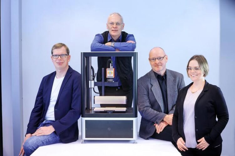
Dr. Philipp Wollmann, Dr. Wulf Grählert, Oliver Throl and Livia Szathmáry (from left) founded the BMWK-funded company "DIVE imaging systems GmbH" to commercialize a promising technology developed at Fraunhofer IWS.
© Amac Garbe/Fraunhofer IWS
“DIVE imaging systems” Spins off from Fraunhofer IWS in Dresden.
Precise two-dimensional analysis of high-tech layers in microelectronics, battery factories or even in the automotive sector approaches within reach. A measuring system developed at the Fraunhofer Institute for Material and Beam Technology IWS facilitates this by integrating hyperspectral sensor technology, artificial intelligence and special illumination techniques into a high-performance, highly flexible inspection system. A team of researchers from Fraunhofer IWS establishes “DIVE imaging systems GmbH”, a BMWK-funded spin-off company, to commercialize this promising technology.
DIVE (short for “Digital Vision Experts”) will initially focus on the semiconductor industry. In this industry, the founders Dr. Philipp Wollmann, Dr. Wulf Grählert, Oliver Throl, and Livia Szathmáry strive to help ensuring stable processes, increasing yields, and saving resources. By no means was the choice of location random: “Dresden is predestined for our spin-off,” emphasizes Philipp Wollmann. “Important players in microelectronics are concentrated here in a metropolitan area. In order to further develop our technology in the best possible customer-oriented way, we enjoy the shortest distances in this city and can also identify further partners with the successive expansion of the already existing network.”
The founders think not only of customers from the semiconductor industry. In perspective, the quartet wants to establish its innovative DIVE technology for the inspection and analysis of surfaces and layers broadly in different industries. Of the numerous scenarios, rapid areal layer thickness measurement, the detection and localization of the smallest form defects or impurities represent only a fraction of the possibilities.
Light Dispersed into 1000 Colors
The DIVE system uses visible light and invisible infrared thermal radiation in frequencies between 0.4 and 2.5 micrometers (thousandths of a millimeter) to illuminate the silicon wafers from which microchips for laptops, cell phones, cars, etc. are manufactured in semiconductor fabs around the world. A special so-called hyperspectral camera records the reflected light. While the human eye, for example, only registers three primary colors – red, green, blue – the hyperspectral camera distinguishes up to 1000 “colors” or wavelengths of light. The high-dimensional raw data, which can quickly grow to several gigabytes, is then forwarded to an artificial intelligence (AI). This AI can use the “1000-color image” to detect possible damage or contamination, as well as evaluate the quality of individual chips or the entire wafer. The DIVE system can thus detect, for example, whether the coating step on the wafer has been successful, and determine the layer’s homogeneity, thinness, evenness, or lack of defects. This ensures only flawless wafers to enter the subsequent production steps.
Kick-off Project with the German Chip Group Infineon
Already today, monitoring of the wafers in the semiconductor factories takes place during the many production steps up to the final microchip with regard to many properties. However, the analysis of entire wafer area is comparably slow and is therefore carried out sampled.
DIVE comes into play at this point: Together with the semiconductor manufacturer Infineon, the team will first develop a hyperspectral system for laboratories beyond the clean room and, in a next step, a system suitable for use in such a laboratory. In the future, DIVE plans to develop an inline solution for direct integration into cleanroom facilities. This will allow real-time analysis of many process steps.
Given the great potential of this technology, the four-member team expects rapid growth. Indeed, the founders contribute several unique selling propositions from Fraunhofer IWS: These include the complete system concept including sample illumination as well as the sophisticated software for system control and for AI-supported data analysis. DIVE will manufacture the designed devices, systems and later entire system components itself in its own production line. The team will also provide services, technical assistance and customized developments. The spin-off is receiving significant support from the German Federal Ministry for Economic Affairs and Climate (BMWK), which is providing 18 months of funding worth 1.2 million euros as part of an EXIST research transfer program.
New Look at Old Books Possible
After the spin-off, Fraunhofer IWS will continue to intensively develop hyperspectral technology in different directions. For example, the research agenda includes concepts that use a laser to illuminate samples or drastically miniaturize hyperspectral systems. The researchers also want to use algorithms to extract significantly more information from raw data. In the future, many other economic and social application scenarios should develop from these approaches, such as the further development of hyperspectral technology for libraries in order to transfer valuable, highly sensitive cultural assets into a public available digital form. In the future, digital twins could be created that store a variety of data in addition to traditional image and font information, such as paper thickness and type, document age, or color pigments used.
Precisely this transfer of know-how into practice forms the focus of attention at the Dresden Institute time and again. Transferring cutting-edge research results into commercial practice quickly and in a customer-oriented manner originates from the Fraunhofer DNA. “To be specific, we are transferring a technology portfolio that has been developed at Fraunhofer IWS for more than ten years with enormous potential,” Philipp Wollmann summarizes. “We will help the semiconductor industry in Germany and Europe to process wafers particularly efficiently as well as with high quality and yield. In this way, we are also supporting the EU’s goals of significantly increasing the share of European microelectronics in the world market. On the other hand, we are thus securing jobs and value creation in the region.”
Further information:
https://s.fhg.de/iws-dive-en
About DIVE
DIVE imaging systems GmbH, a Fraunhofer IWS spin-off, defines a new class of machine vision for surface and layer inspection. DIVE’s “hyperspectral vision devices” synergistically combine the advantages of classical imaging with spectroscopic analysis of chemical-physical properties, including artificial intelligence-based data analysis. These innovative inspection systems enable users to “see” and objectively evaluate previously hidden properties of surfaces and coating systems. DIVE technology automates quality control, reduces inspection time and increases manufacturing quality.
More information:
www.dive.eu
Infobox
Hyperspectral Cameras
The hyperspectral principle was first used in the 1970s for satellite-based remote sensing of the Earth’s surface. While the multispectral cameras of that time could only split the sunlight reflected by the earth into four to six color bands, today’s hyperspectral cameras resolve the light into up to 1000 color or frequency bands.
Wissenschaftliche Ansprechpartner:
Dr. rer. nat. Philipp Wollmann
CEO
DIVE imaging systems GmbH
Winterbergstraße 28, DE-01277 Dresden
www.dive.eu
philipp@dive.com.de
Phone +49 351 83391-3316
Originalpublikation:
https://www.iws.fraunhofer.de/en/newsandmedia/press_releases/2023/press-release_…
Media Contact
All latest news from the category: Machine Engineering
Machine engineering is one of Germany’s key industries. The importance of this segment has led to the creation of new university degree programs in fields such as production and logistics, process engineering, vehicle/automotive engineering, production engineering and aerospace engineering among others.
innovations-report offers informative reports and articles covering technologies such as automation, motion, power train, energy, conveyor, plastics, lightweight construction, logistics/warehousing, measurement systems, machine tools and control engineering.


Newest articles

Faster, more energy-efficient way to manufacture an industrially important chemical
Zirconium combined with silicon nitride enhances the conversion of propane — present in natural gas — needed to create in-demand plastic, polypropylene. Polypropylene is a common type of plastic found…

Energy planning in Ghana as a role model for the world
Improving the resilience of energy systems in the Global South. What criteria should we use to better plan for resilient energy systems? How do socio-economic, technical and climate change related…

Artificial blood vessels could improve heart bypass outcomes
Artificial blood vessels could improve heart bypass outcomes. 3D-printed blood vessels, which closely mimic the properties of human veins, could transform the treatment of cardiovascular diseases. Strong, flexible, gel-like tubes…

