Layered graphene with a twist displays unique quantum confinement in 2-D
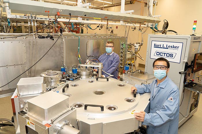
Staff scientist Jurek Sadowski (left) and postdoc Zhongwei Dai at the Quantum Material Press (QPress) facility at the Center for Functional Nanomaterials (CFN) at Brookhaven National Laboratory. The large circular piece is the central QPress robot, with various modules attached on the sides for sample annealing, film deposition, plasma cleaning, and sample libraries. The full QPress system, still under development, will automate the stacking of 2-D materials into layered structures with exotic properties for quantum applications.
Credit: Brookhaven National Laboratory / Usage Restrictions: https://www.bnl.gov/newsroom/image-use.php
Understanding how electrons move in 2-D layered material systems could lead to advances in quantum computing and communication.
Scientists studying two different configurations of bilayer graphene—the two-dimensional (2-D), atom-thin form of carbon—have detected electronic and optical interlayer resonances. In these resonant states, electrons bounce back and forth between the two atomic planes in the 2-D interface at the same frequency. By characterizing these states, they found that twisting one of the graphene layers by 30 degrees relative to the other, instead of stacking the layers directly on top of each other, shifts the resonance to a lower energy. From this result, just published in Physical Review Letters, they deduced that the distance between the two layers increased significantly in the twisted configuration, compared to the stacked one. When this distance changes, so do the interlayer interactions, influencing how electrons move in the bilayer system. An understanding of this electron motion could inform the design of future quantum technologies for more powerful computing and more secure communication.
“Today’s computer chips are based on our knowledge of how electrons move in semiconductors, specifically silicon,” said first and co-corresponding author Zhongwei Dai, a postdoc in the Interface Science and Catalysis Group at the Center for Functional Nanomaterials (CFN) at the U.S. Department of Energy (DOE)’s Brookhaven National Laboratory. “But the physical properties of silicon are reaching a physical limit in terms of how small transistors can be made and how many can fit on a chip. If we can understand how electrons move at the small scale of a few nanometers in the reduced dimensions of 2-D materials, we may be able to unlock another way to utilize electrons for quantum information science.”
At a few nanometers, or billionths of a meter, the size of a material system is comparable to that of the wavelength of electrons. When electrons are confined in a space with dimensions of their wavelength, the material’s electronic and optical properties change. These quantum confinement effects are the result of quantum mechanical wave-like motion rather than classical mechanical motion, in which electrons move through a material and are scattered by random defects.
For this research, the team selected a simple material model—graphene—to investigate quantum confinement effects, applying two different probes: electrons and photons (particles of light). To probe both electronic and optical resonances, they used a special substrate onto which the graphene could be transferred. Co-corresponding author and CFN Interface Science and Catalysis Group scientist Jurek Sadowski had previously designed this substrate for the Quantum Material Press (QPress). The QPress is an automated tool under development in the CFN Materials Synthesis and Characterization Facility for the synthesis, processing, and characterization of layered 2-D materials. Conventionally, scientists exfoliate 2-D material “flakes” from 3-D parent crystals (e.g., graphene from graphite) on a silicon dioxide substrate several hundred nanometers thick. However, this substrate is insulating, and thus electron-based interrogation techniques don’t work. So, Sadowski and CFN scientist Chang-Yong Nam and Stony Brook University graduate student Ashwanth Subramanian deposited a conductive layer of titanium oxide only three nanometers thick on the silicon dioxide substrate.
“This layer is transparent enough for optical characterization and determination of the thickness of exfoliated flakes and stacked monolayers while conductive enough for electron microscopy or synchrotron-based spectroscopy techniques,” explained Sadowski.
In the Charlie Johnson Group at the University of Pennsylvania—Rebecca W. Bushnell Professor of Physics and Astronomy Charlie Johnson, postdoc Qicheng Zhang, and former postdoc Zhaoli Gao (now an assistant professor at the Chinese University of Hong Kong)—grew the graphene on metal foils and transferred it onto the titanium oxide/silicon dioxide substrate. When graphene is grown in this way, all three domains (single layer, stacked, and twisted) are present.
Then, Dai and Sadowski designed and carried out experiments in which they shot electrons into the material with a low-energy electron microscope (LEEM) and detected the reflected electrons. They also fired photons from a laser-based optical microscope with a spectrometer into the material and analyzed the spectrum of light scattered back. This confocal Raman microscope is part of the QPress cataloger, which together with image-analysis software, can pinpoint the locations of sample areas of interest.
“The QPress Raman microscope enabled us to quickly identify the target sample area, accelerating our research,” said Dai.
Their results suggested that the spacing between layers in the twisted graphene configuration increased by about six percent relative to the non-twisted configuration. Calculations by theorists at the University of New Hampshire verified the unique resonant electronic behavior in the twisted configuration.
“Devices made out of rotated graphene may have very interesting and unexpected properties because of the increased interlayer spacing in which electrons can move,” said Sadowski.
Next, the team will fabricate devices with the twisted graphene. The team will also build upon initial experiments conducted by CFN staff scientist Samuel Tenney and CFN postdocs Calley Eads and Nikhil Tiwale to explore how adding different materials to the layered structure impacts its electronic and optical properties.
“In this initial research, we picked the simplest 2-D material system we can synthesize and control to understand how electrons behave,” said Dai. “We plan to continue these types of fundamental studies, hopefully shedding light on how to manipulate materials for quantum computing and communications.”
This research was supported by the DOE Office of Science and used resources of the CFN and National Synchrotron Light Source II (NSLS-II), both DOE Office of Science User Facilities at Brookhaven. The LEEM microscope is part of the x-ray photoemission electron microscopy (XPEEM)/LEEM endstation of the Electron Spectro-Microscopy beamline at NSLS-II; the CFN operates this endstation through a partner user agreement with NSLS-II. The other funding agencies are the National Science Foundation, Research Grant Council of Hong Kong Special Administrative Region, and the Chinese University of Hong Kong.
Brookhaven National Laboratory is supported by the U.S. Department of Energy’s Office of Science. The Office of Science is the single largest supporter of basic research in the physical sciences in the United States and is working to address some of the most pressing challenges of our time. For more information, visit https://energy.gov/science.
Follow @BrookhavenLab on Twitter or find us on Facebook.
Journal: Physical Review Letters
DOI: 10.1103/PhysRevLett.127.086805
Subject of Research: Not applicable
Article Title: Quantum-Well Bound States in Graphene Heterostructure Interfaces
Article Publication Date: 20-Aug-2021
Media Contact
Ariana Manglaviti
amanglaviti@bnl.gov
Office: 631-344-2347
Media Contact
All latest news from the category: Information Technology
Here you can find a summary of innovations in the fields of information and data processing and up-to-date developments on IT equipment and hardware.
This area covers topics such as IT services, IT architectures, IT management and telecommunications.


Newest articles

A universal framework for spatial biology
SpatialData is a freely accessible tool to unify and integrate data from different omics technologies accounting for spatial information, which can provide holistic insights into health and disease. Biological processes…

How complex biological processes arise
A $20 million grant from the U.S. National Science Foundation (NSF) will support the establishment and operation of the National Synthesis Center for Emergence in the Molecular and Cellular Sciences (NCEMS) at…

Airborne single-photon lidar system achieves high-resolution 3D imaging
Compact, low-power system opens doors for photon-efficient drone and satellite-based environmental monitoring and mapping. Researchers have developed a compact and lightweight single-photon airborne lidar system that can acquire high-resolution 3D…

