A performance leap for Graphene modulators in next generation datacom and telecom
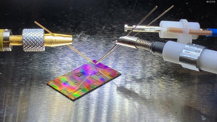
Graphene-based electro-absorption modulator chip under study in the lab.
Credit: ©ICFO
Over the past years, global data traffic has experienced a boom, with over 12.5 billion connected devices all over the world. The current world-wide deployment of the 5G telecommunications standard is triggering the need for smaller devices with enhanced performances, such as higher speed, lower power consumption and reduced cost as well as easier manufacturability.
In search for the appropriate technology, photonic devices emerged as the leading technology for the evolution of such information and communication technologies, already surpassing the capabilities of current microelectronics and CMOS technologies.
Optical communication systems rely on three basic components: modulators, waveguides and photodetectors. The modulation of light is key for photonic integrated circuits because it allows to transmit multiple signals simultaneously over a single channel. More specifically, electro-absorption (EA) modulators modulate the amplitude of the light passing through the optical waveguide.
So far, silicon and graphene are winning the race since they are proving to be the most scalable, cost-effective and CMOS compatible materials for optical modulation and detection. Graphene-based modulators have already shown broadband optical bandwidth and temperature stability, but in occasions, they have been incapable of showing both high-speed and high modulation efficiencies simultaneously, due to the limited quality of graphene and a combination between the graphene and the dielectric material.
Now, in a study published in Nature Communications, ICFO researchers Hitesh Agarwal, Bernat Terrés, Lorenzo OrsinI, led by ICREA Professor at ICFO Frank Koppens, in collaboration with researchers from Universita di Pisa, CNIT, Ghent University-IMEC, and NIMS have reported on a novel EA modulator capable of showing a 3-fold increase in static and dynamic modulation efficiency while maintaining the high-speed, a value that surpasses those for previously reported graphene EA modulators.
To achieve this, the team of researchers developed a high-quality graphene-based electro-absorption modulator by combining high-quality graphene and a high-k dielectric, also used in microelectronics. The high quality of the graphene was achieved by integrating it with the 2d-material dielectric hexagonal boron nitride (hBN). Interestingly enough, the team was then able to add the high-k dielectric material HfO2 sandwiched in between two layers of boron nitride, which permitted operating with much smaller voltages, and, at the same time, achieving symmetric and hysteresis-free due to the high quality of the graphene. By doing this, the dielectric combination was able to enhance the EA modulator capacitance without compromising the robustness of the device against high voltages, preserve the high mobility of charge carries (increasing the modulation efficiency) while maintaining low levels of doping.
As Hitesh Agarwal, researcher at ICFO and first author of the study, comments, “Because one of the major bottlenecks for the integration of graphene into CMOS fab lines is its incompatibility with high-k oxides, this motivated us to build the structure of hBN-HfO2-hBN. Not only we managed to achieve high modulation efficiency (due to high-K dielectric), but also higher speed (due to increased mobility).”
“We have been waiting for a while to see the outstanding fundamental capabilities of graphene to unleash in applications”, Bernat Terrés, Postdoc researcher at ICFO and corresponding author of the work, adds. He also stresses that “Optoelectronics is one of the first where this 2D material overcomes current state-of-the-art technologies, bringing an encouraging prospect for other commercial applications”.
In summary, the device was capable of outperforming previous modulators, operating at high-speeds while, maintaining a very high modulation efficiency, low power consumption, achieving a record breaking 39GHz bandwidth, with operations up to 40Gbps speed, and consequently overcoming the fundamental limitations obtained so far with double layer graphene systems.
The compatibility of this device with silicon technology and microelectronics could facilitate the scaling improvements that we face nowadays for the photonic industry as well as implement this type of technology for a much greater range of functionalities in electronic and optoelectronic applications. Such results could definitely benefit applications for high-speed and low-latency optical networks such as autonomous vehicles, remote surgery, IoT, to name a few.
Collaborator of the study, Marco Romagnoli, researcher at CNIT and work-package leader of the Graphene Flagship, comments, “This new scientific result of ultrafast electro absorption modulator paves the way towards the continuous race for speed demonstrating the highest electro-optical bandwidth achieved with graphene and 2D materials. In addition, this work is also the first example of full 3D integration entirely realized by assembling different types of 2D materials demonstrating the potentiality of these new routes in microfabrication of integrated circuits.”
In addition, Wolfgang Templ, from Nokia Bell Labs highlights “This work shows that the discussed 2D-3D dielectric integration of high-quality double layer encapsulated Graphene structures can open the way to the realisation of new high performing and micro-sized electro absorption modulators (EAMs) which can be combined with Si-based electronic into most advanced highly integrated photonic circuits”.
Finally, Frank Koppens, ICREA Professor at ICFO and work-package leader of the Graphene Flagship, pinpoints “Data traffic is growing rapidly and will benefit society greatly, for example by enabling autonomous vehicles. The power consumption of high data traffic rates, however, is a key challenge that needs to be addressed. I’m happy to see that graphene-based modulators with much lower power consumption, as shown in this work, can tackle two societal challenges at the same time.”
###
Link to the paper: https:/
Link to the research group led by ICREA Prof at ICFO Frank Koppens: https:/
Link to graphene at ICFO: http://graphene.
Link to the graphene Flagship: https:/
All latest news from the category: Information Technology
Here you can find a summary of innovations in the fields of information and data processing and up-to-date developments on IT equipment and hardware.
This area covers topics such as IT services, IT architectures, IT management and telecommunications.


Newest articles

A universal framework for spatial biology
SpatialData is a freely accessible tool to unify and integrate data from different omics technologies accounting for spatial information, which can provide holistic insights into health and disease. Biological processes…

How complex biological processes arise
A $20 million grant from the U.S. National Science Foundation (NSF) will support the establishment and operation of the National Synthesis Center for Emergence in the Molecular and Cellular Sciences (NCEMS) at…

Airborne single-photon lidar system achieves high-resolution 3D imaging
Compact, low-power system opens doors for photon-efficient drone and satellite-based environmental monitoring and mapping. Researchers have developed a compact and lightweight single-photon airborne lidar system that can acquire high-resolution 3D…

