Electronic Highways on the Nanoscale
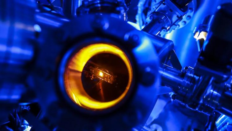
In the Laboratory a structured silicon carbide crystal is heated in a preparation chamber of a scanning tunneling microscope, so that small graphene structures can be formed. Photo: TU Chemnitz/Jacob Müller
Computers are getting faster and increasingly powerful. However, at the same time computing requires noticeably more energy, which is almost completely converted to wasted heat. This is not only harmful to the environment, but also limits further miniaturization of electronic components and increase of clock rates.
A way out of this dilemma are conductors with no electrical resistance. Based on carbon nanostructures, such conductors can be realized. By applying sophisticated heating processes to nanostructured silicon carbide crystals, small graphene structures, so-called graphene nanoribbons, can be produced at their edges. Graphene is a single layer of carbon atoms arranged in a honeycomb lattice.
Physicists at the Chemnitz University of Technology in collaboration with researchers from the University of Twente (Netherlands) and the MAX IV Laboratory in Lund (Sweden) succeeded now to produce and to characterize such so-called ballistic wires.
“The intriguing property of such conductors is that the electrons pass through these tiny wires without heating them – ideally irrespective of the wire length,” explains Prof. Dr. Christoph Tegenkamp, chair of the Department of Analytics of Solid Surfaces at the Chemnitz University of Technology. In a variety of complex experiments including atomic force and multi-tip scanning tunneling microscopy, the adjacent quantum transport channels were measured in detail and even imaged directly at room temperature and atmosphere on the nanoscale.
“Surprisingly, we could now even identify several spatially separated channels on one wire that apparently do not influence each other”, explains Johannes Aprojanz, who is currently working on this research topic at the Chemnitz University of Technology in his doctoral thesis.
In cooperation with theorists from Copenhagen and Barcelona, this unique effect has been traced back to an asymmetric interaction of the edges with the substrate, as reported in the journal Nature Communication in its current issue. The authors of the study are sure that this type of functionalization is also interesting for topological effects in other 2D materials and shows new ways for the design of future quantum devices. “We are opening the door a bit wider for computers that are hardly warming up”, said Tegenkamp.
Prof. Dr. Christoph Tegenkamp, Tel. +49 371 531-33103, E-mail christoph.tegenkamp@physik.tu-chemnitz.de.
https://www.nature.com/articles/s41467-018-06940-5
https://www.tu-chemnitz.de/physik/AFKO/index.html.en – Homepage for the Department of Analytics of Solid Surfaces
Media Contact
All latest news from the category: Materials Sciences
Materials management deals with the research, development, manufacturing and processing of raw and industrial materials. Key aspects here are biological and medical issues, which play an increasingly important role in this field.
innovations-report offers in-depth articles related to the development and application of materials and the structure and properties of new materials.


Newest articles

A universal framework for spatial biology
SpatialData is a freely accessible tool to unify and integrate data from different omics technologies accounting for spatial information, which can provide holistic insights into health and disease. Biological processes…

How complex biological processes arise
A $20 million grant from the U.S. National Science Foundation (NSF) will support the establishment and operation of the National Synthesis Center for Emergence in the Molecular and Cellular Sciences (NCEMS) at…

Airborne single-photon lidar system achieves high-resolution 3D imaging
Compact, low-power system opens doors for photon-efficient drone and satellite-based environmental monitoring and mapping. Researchers have developed a compact and lightweight single-photon airborne lidar system that can acquire high-resolution 3D…

