Clarification of a new synthesis mechanism of semiconductor atomic sheet
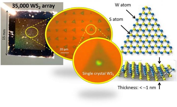
A substrate (left photograph) that is fabricated by integrating about 35,000 monolayer single crystals of WS2, and a structural schematic of the monolayer single crystal of WS2 (right figure). Credit: ©Toshiaki Kato
In Japan Science and Technology Agency's Strategic Basic Research Programs, Associate Professor Toshiaki Kato and Professor Toshiro Kaneko of the Department of Electronic Engineering, Graduate School of Engineering, Tohoku University succeeded in clarifying a new synthesis mechanism regarding transition metal dichalcogenides (TMD)1), which are semiconductor atomic sheets having thickness in atomic order.
Because it is difficult to directly observe the aspect of the growing process of TMD in a special environment, the initial growth process remained unclear, and it has been desirable to elucidate a detailed mechanism of synthesis to obtain high-quality TMD.
An in-situ observing synthesis method2) has been developed by our research group to examine the growth aspect of TMD as a real-time optical image in a special high temperature atmosphere of about 800°C in the presence of corrosive gases.
In addition, a synthesis substrate, which is a mechanism to control diffusion during the crystal growth of a precursor3), has been developed in advance; further, it has been clarified that the growing precursor diffuses a distance about 100 times larger than in conventional semiconductor materials.
It was also demonstrated that nucleation occurs due to the involvement of the precursor in a droplet state. Furthermore, by utilizing this method, a large-scale integration of more than 35,000 monolayer single crystal atomic sheets has been achieved on a substrate in a practical scale (Figure 1).
Utilizing the results of the present research, the large-scale integration of atomic-order thick4) semiconductor atomic sheets can be fabricated and is expected to be put into practical use in the field of next-generation flexible electronics.
###
Notes
1) Transition Metal Dichalcogenides: TMD
Atomic layer materials are similar to graphene. This material has a structure in which a transition metal is sandwiched between the chalcogen atoms. Graphene shows metallic conduction characteristics but TMD has a band gap to show semiconductor properties and is expected to be applied in the field of semiconductor devices.
2) In-situ monitoring synthesis method
A crystal growing technique capable of monitoring the synthesis states in real time.
3) Precursor
Raw material for crystal growing. When incorporated into the crystal, a part or all of it becomes an element constituting the crystal.
4) Atomic order
The size of one atom is about several angstroms (one angstrom is one ten billionth of a meter). This means the size of one to several integrated atoms.
Media Contact
All latest news from the category: Materials Sciences
Materials management deals with the research, development, manufacturing and processing of raw and industrial materials. Key aspects here are biological and medical issues, which play an increasingly important role in this field.
innovations-report offers in-depth articles related to the development and application of materials and the structure and properties of new materials.


Newest articles

High-energy-density aqueous battery based on halogen multi-electron transfer
Traditional non-aqueous lithium-ion batteries have a high energy density, but their safety is compromised due to the flammable organic electrolytes they utilize. Aqueous batteries use water as the solvent for…

First-ever combined heart pump and pig kidney transplant
…gives new hope to patient with terminal illness. Surgeons at NYU Langone Health performed the first-ever combined mechanical heart pump and gene-edited pig kidney transplant surgery in a 54-year-old woman…

Biophysics: Testing how well biomarkers work
LMU researchers have developed a method to determine how reliably target proteins can be labeled using super-resolution fluorescence microscopy. Modern microscopy techniques make it possible to examine the inner workings…

