Hannover Messe: TCO inks allow direct printing of transparent conductor structures on film
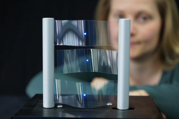
TCO inks allow direct printing of transparent conductor structures on film. Copyright: Uwe Bellhäuser, only free within this press release.
TCOs are normally produced using vacuum coating such as sputtering. At the INM, special TCO inks have been developed for the wet-chemical application of TCO layers to both solid and flexible substrates, such as plastic film.
To do this, developers at the INM use TCO inks containing TCO nanoparticles and produced using wet chemistry processes. This method enables not only application to plastics and films but also, for the first time, direct printing of transparent conductor structures.
From 7 to 11 April 2014, the researchers of the INM will be presenting this and further results in Hall 2 at the stand C48 of the Hannover Messe in the context of the leading trade fair for R&D and Technology Transfer.
“We produce special nanoparticles from the transparent conducting oxides”, explains Peter William de Oliveira, Head of the Optical Materials Program Division. “By adding a solvent and a special binder, these modified TCO nanoparticles can be applied to the film directly by gravure printing as an “ink” using a printing plate”, he adds.
This process has a number of advantages. Gravure printing enables TCO layers to be printed cost-effectively in just one process step. As a result of UV curing at temperatures below 150°C, it is also possible to coat thin plastic films.
The binder fulfills a number of tasks here. It produces good adhesion of the TCO nanoparticles to the substrate and also increases the flexibility of the TCO layers. This means that the conductivity remains the same, even if the films become distorted – a clear advantage over current high-vacuum techniques such as sputtering.
“There is still potential here for further development”, explains physicist de Oliveira. “If we succeed in also making the binder conductive, conductivity as a whole will increase and the surface resistance will be further reduced.”
Coating on flexible film substrates is possible using the classic roll-to-roll process. Initial experiments on this at the INM are promising, and researchers are agreed that the use of structured rolls in future will mean that large, structured, conductive surfaces can also be printed cost-effectively and with a high output.
In addition to using TCO nanoparticles, developers at the INM are also working with the wet chemistry sol-gel process which is particularly suitable for temperature-stable substrates such as glass or ceramic. In this process, curing takes place at temperatures above 450°C. In addition to large-area substrates, more complex geometries such as pipes and moldings can also be coated.
“Here again, the advantage lies in the costs”, says the Head of the Program Division. With vacuum coating processes such as the sputter method, expensive high-vacuum apparatus and large TCO targets are needed for coating large areas; there is also the limited possibility of evenly coating curved substrates using this technique.
At the INM, too, the material of choice is predominantly indium tin oxide (ITO). Because of dwindling resources and the high price of the raw material indium, researchers at the INM are also increasingly testing alternative transparent oxides such as aluminum zinc oxide (AZO).
Contact:
Dr. Peter William de Oliveira
INM – Leibniz Institute for New Materials
Programme Division Optical Materials
Phone: +49681-9300-148
peter.oliveira@inm-gmbh.de
Your contact at the stand:
Dr. Thomas Müller
Dr. Michael Opsölder
The INM will also present its competence within various talks in Hall 2 at the Tech transfer stand.
* „Nanotechnology at the INM – Leibniz Institute for New Materials“, Dr. Mario Quilitz, Monday, 7.4. 2014, 10:15 – 10:30 a.m.
* „Nanotechnology in the Leibniz Network Nano“, Dr. Mario Quilitz, Monday, 7.4.2014, 12:00 – 12:15 p.m.
* „Nanoparticles for Optics and Electronics“, Dr. Peter William de Oliveira, Tuesday, 8.4.2014, 11:00 – 11:10 a.m.
* „Nanomers – Highly structured integrated functional coatings for practical solutions in industrial applications“, Dr. Carsten Becker-Willinger, Tuesday, 8.4.2014, 11:20 – 11:35 a.m.
INM conducts research and development to create new materials – for today, tomorrow and beyond. Chemists, physicists, biologists, materials scientists and engineers team up to focus on these essential questions: Which material properties are new, how can they be investigated and how can they be tailored for industrial applications in the future? Four research thrusts determine the current developments at INM: New materials for energy application, new concepts for medical surfaces, new surface materials for tribological applications and nano safety and nano bio. Research at INM is performed in three fields: Nanocomposite Technology, Interface Materials, and Bio Interfaces.
INM – Leibniz Institute for New Materials, situated in Saarbruecken, is an internationally leading centre for materials research. It is an institute of the Leibniz Association and has about 195 employees.
Media Contact
All latest news from the category: HANNOVER MESSE


Newest articles
Economies take off with new airports
A global study by an SUTD researcher in collaboration with scientists from Japan explores the economic benefits of airport investment in emerging economies using nighttime satellite imagery. Be it for…
CAR T–cell immunotherapy targets
Pan-cancer analysis uncovers a new class of promising CAR T–cell immunotherapy targets. Scientists at St. Jude Children’s Research Hospital found 156 potential CAR targets across the brain and solid tumors,…

Stony coral tissue loss disease
… is shifting the ecological balance of Caribbean reefs. The outbreak of a deadly disease called stony coral tissue loss disease is destroying susceptible species of coral in the Caribbean…

