Electronic micro and conductor strips for touch screens in the one-step process: Photometallization
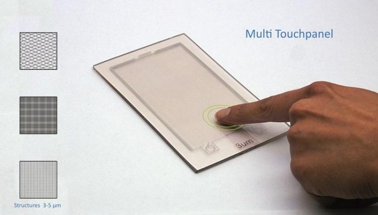
Electronic micro and conductor strips via Photometallization. Copyright: INM
Up to now, these conductor strips have been manufactured in different production stages, but researchers at the INM – Leibniz Institute for New Materials have developed a new process with which they can create macroscopic and microscopic conductor strips in a single production step.
From 7 to 11 April 2014, the researchers of the INM will be presenting this and further results in Hall 2 at the stand C48 of the Hannover Messe in the context of the leading trade fair for R & D and Technology Transfer. This includes new developments for CIGS thin film solar cells, corrosion protection coatings and low-friction coatings as well as antimicrobial coatings and TCO inks.
To produce these conductor strips, the developers give a substrate a photoactive layer consisting of metal oxide nanoparticles. “We then apply a colorless UV-stable silver complex”, explains Peter William de Oliveira, Head of the Optical Materials Program Division. By exposing this series of layers to light, the silver complex on the photoactive layer is broken down and the silver ions reduced to silver. This process offers a number of advantages, including the fact that it is rapid, flexible, low-cost and environmentally friendly.
As there is only one step of exposure to light followed by rinsing with water, production takes just a few minutes. Further process steps for post-treatment are not required; even heat treatment is quite unnecessary. Using this process, researchers at the INM are achieving layers up to 100 nanometers thick and a specific conductivity around a quarter of that of pure silver. Heat treatment at 120°C increases the conductivity to half that of silver.
This basic principle allows researchers at the INM to very individually apply conductor strips of different sizes to substrates such as glass or plastic. “There are three different options that we can use as required. “Writing” using a UV laser is particularly good for the first customized production and testing of a new conductor strip design, but this method is too time-consuming for mass production”, explains physicist de Oliveira.
Photomasks that are only UV-permeable at the desired positions can also be used for structuring. “The production of these masks is quite costly and has a high environmental impact. For a “semi-continuous process” they are particularly suitable for solid substrates such as glass”, says the materials expert, but they were not suitable for a potential roll-to-roll process because they are mainly composed of quartz glass and are not flexible.
The researchers are currently focusing their efforts on a third method using so-called transparent stamps. “These stamps mechanically displace the silver complex, and where there is no silver there is also no conductor strip”, in de Oliveira’s opinion. “So we can form structures measuring just a few micrometers. Since the stamps are made of a flexible polymer, we have here the possibility of arranging them on a roll. Because they are transparent, we are working on incorporating the UV source in the roll, so the first steps would be done for a roll-to-roll process”, the Head of the Program Division sums up. This has enabled conductor strip structures of different sizes to be produced on substrates such as polyethylene or polycarbonate film on a large scale.
Contact:
Dr. Peter William de Oliveira
INM – Leibniz Institute for New Materials
Head Optical Materials
Phone: +49681-9300-148
peter.oliveira@inm-gmbh.de
Your contact at the stand:
Dr. Thomas Müller
Dr. Michael Opsölder
The INM will also present its competence within various talks in Hall 2 at the Tech transfer stand.
* „Nanotechnology at the INM – Leibniz Institute for New Materials“, Dr. Mario Quilitz, Monday, 7.4. 2014, 10:15 – 10:30 a.m.
* „Nanotechnology in the Leibniz Network Nano“, Dr. Mario Quilitz, Monday, 7.4.2014, 12:00 – 12:15 p.m.
* „Nanoparticles for Optics and Electronics“, Dr. Peter William de Oliveira, Tuesday, 8.4.2014, 11:00 – 11:10 a.m.
* „Nanomers – Highly structured integrated functional coatings for practical solutions in industrial applications“, Dr. Carsten Becker-Willinger, Tuesday, 8.4.2014, 11:20 – 11:35 a.m.
INM conducts research and development to create new materials – for today, tomorrow and beyond. Chemists, physicists, biologists, materials scientists and engineers team up to focus on these essential questions: Which material properties are new, how can they be investigated and how can they be tailored for industrial applications in the future? Four research thrusts determine the current developments at INM: New materials for energy application, new concepts for medical surfaces, new surface materials for tribological applications and nano safety and nano bio. Research at INM is performed in three fields: Nanocomposite Technology, Interface Materials, and Bio Interfaces.
INM – Leibniz Institute for New Materials, situated in Saarbruecken, is an internationally leading centre for materials research. It is an institute of the Leibniz Association and has about 195 employees.
Media Contact
All latest news from the category: HANNOVER MESSE


Newest articles
Insect research is revolutionized by technology
New technologies can revolutionise insect research and environmental monitoring. By using DNA, images, sounds and flight patterns analysed by AI, it’s possible to gain new insights into the world of…

Expanding a lymph node, boosting a vaccine
A biomaterial vaccine enhances and sustains lymph node expansion following vaccination, boosting anti-tumor immunity in an animal model. Each one of us has around 600 lymph nodes (LNs) – small,…

AI to Make Crop Production More Sustainable
Drones monitoring fields for weeds and robots targeting and treating crop diseases may sound like science fiction but is actually happening already, at least on some experimental farms. Researchers from…

