Researchers Advance Scheme to Design Seamless Integrated Circuits Etched on Graphene
<br>
Researchers in electrical and computer engineering at UC Santa Barbara have introduced and modeled an integrated circuit design scheme in which transistors and interconnects are monolithically patterned seamlessly on a sheet of graphene, a 2-dimensional plane of carbon atoms. The demonstration offers possibilities for ultra energy-efficient, flexible, and transparent electronics.
Bulk materials commonly used to make CMOS transitors and interconnects pose fundamental challenges in continuous shrinking of their feature-sizes and suffer from increasing “contact resistance” between them, both of which lead to degrading performance and rising energy consumption. Graphene-based transistors and interconnects are a promising nanoscale technology that could potentially address issues of traditional silicon-based transistors and metal interconnects.
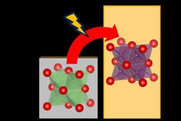
“In addition to its atomically thin and pristine surfaces, graphene has a tunable band gap, which can be adjusted by lithographic sketching of patterns – narrow graphene ribbons can be made semiconducting while wider ribbons are metallic. Hence, contiguous graphene ribbons can be envisioned from the same starting material to design both active and passive devices in a seamless fashion and lower interface/contact resistances,” explained Kaustav Banerjee, professor of electrical and computer engineering and director of the Nanoelectronics Research Lab at UCSB. Banerjee's research team also includes UCSB researchers Jiahao Kang, Deblina Sarkar and Yasin Khatami. Their work was recently published in the journal Applied Physics Letters.
“Accurate evaluation of electrical transport through the various graphene nanoribbon based devices and interconnects and across their interfaces was key to our successful circuit design and optimization,” explained Jiahao Kang, a PhD student in Banerjee's group and a co-author of the study. Banerjee's group pioneered a methodology using the Non-Equilibrium Green's Function (NEGF) technique to evaluate the performance of such complex circuit schemes involving many heterojunctions. This methodology was used in designing an “all-graphene” logic circuit reported in this study.
“This work has demonstrated a solution for the serious contact resistance problem encounterd in conventional semiconductor technology by providing an innovative idea of using an all-graphene device-interconnect scheme. This will significantly simplify the IC fabrication process of graphene based nanoelectronic devices.” commented Philip Kim, professor of physics at Columbia University, and a renowned scientist in the graphene world.
As reported in their study, the proposed all-graphene circuits have achieved 1.7X higher noise margins and 1-2 decades lower static power consumption over current CMOS technology. According to Banerjee, with the ongoing worldwide efforts in patterning and doping of graphene, such circuits can be realized in the near future.
“We hope that this work will encourage and inspire other researchers to explore graphene and beyond-graphene emerging 2-dimensional crystals for designing such ‘band-gap engineered' circuits in the near future,” added Banerjee.
Their research was supported by the National Science Foundation.
The College of Engineering at University of California, Santa Barbara is recognized globally as a leader among the top tier of engineering education and research programs, and is renowned for a successful interdisciplinary approach to engineering research.
Media Contact
Melissa Van De Werfhorst
melissa@engineering.ucsb.edu
Media Contact
More Information:
http://www.ucsb.eduAll latest news from the category: Physics and Astronomy
This area deals with the fundamental laws and building blocks of nature and how they interact, the properties and the behavior of matter, and research into space and time and their structures.
innovations-report provides in-depth reports and articles on subjects such as astrophysics, laser technologies, nuclear, quantum, particle and solid-state physics, nanotechnologies, planetary research and findings (Mars, Venus) and developments related to the Hubble Telescope.


Newest articles

Webb captures top of iconic horsehead nebula in unprecedented detail
NASA’s James Webb Space Telescope has captured the sharpest infrared images to date of a zoomed-in portion of one of the most distinctive objects in our skies, the Horsehead Nebula….
Cost-effective, high-capacity, and cyclable lithium-ion battery cathodes
Charge-recharge cycling of lithium-superrich iron oxide, a cost-effective and high-capacity cathode for new-generation lithium-ion batteries, can be greatly improved by doping with readily available mineral elements. The energy capacity and…

Novel genetic plant regeneration approach
…without the application of phytohormones. Researchers develop a novel plant regeneration approach by modulating the expression of genes that control plant cell differentiation. For ages now, plants have been the…

