3D Plasmonic Antenna Capable of Focusing Light into Few Nanometers
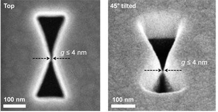
Figure 1: 3D Gap-Plasmon Antenna Structure and the Simulation Results Copyright : KAIST
Professors Myung-Ki Kim and Yong-Hee Lee of the Physics Department at KAIST and their research teams developed a 3D gap-plasmon antenna which can focus light into a few nanometers wide space. Their research findings were published in the June 10th issue of Nano Letters.
Focusing light into a point-like space is an active research field as it finds many applications. However, concentrating light into a smaller space than its wavelength is often hindered by diffraction. In order to tackle this problem, many researchers have utilized the plasmonic phenomenon in a metal where light can be confined to a greater extent by overcoming the diffraction limit.
Many researchers focused on developing a two dimensional plasmonic antenna and were able to focus light under 5 nanometers. However, this two dimensional antenna reveals a challenge that the light disperses to the opposite end regardless of how small it was focused. For a solution, a three dimensional structure has to be employed in order to maximize the light intensity.
Adopting the proximal focused-ion-beam milling technology, the KAIST research team developed a three dimensional 4 nanometer wide gap-plasmon antenna. By squeezing the photons into a three dimensional nano space of 4 x 10 x 10 nm3 size, the researchers were able to increase the intensity of light 400,000 times stronger than that of the incident light.
Capitalizing on the enhanced intensity of light within the antenna, they intensified the second-harmonic signal and verified that the light was focused in the nano gap by scanning cathodoluminescence images.
This technology is expected to improve the speed of data transfer and processing up to the level of terahertz (one trillion times per second) and to enlarge the storage volume per unit area on hard disks by 100 times. In addition, high definition images of sub-molecule size can be taken with actual light, instead of using an electron microscope, while it can improve the semiconductor process to a smaller size of few nanometers.
Professor Kim said, “A simple yet genuine idea has shifted the research paradigm from 2D gap-plasmon antennas to 3D antennas. This technology sees numerous applications including in the field of information technology, data storage, image medical science, and semiconductor process.”
The research was sponsored by the National Research Foundation of Korea.
Associated links
KAIST article
Media Contact
More Information:
http://www.researchsea.comAll latest news from the category: Physics and Astronomy
This area deals with the fundamental laws and building blocks of nature and how they interact, the properties and the behavior of matter, and research into space and time and their structures.
innovations-report provides in-depth reports and articles on subjects such as astrophysics, laser technologies, nuclear, quantum, particle and solid-state physics, nanotechnologies, planetary research and findings (Mars, Venus) and developments related to the Hubble Telescope.


Newest articles

Detector for continuously monitoring toxic gases
The material could be made as a thin coating to analyze air quality in industrial or home settings over time. Most systems used to detect toxic gases in industrial or…

On the way for an active agent against hepatitis E
In order to infect an organ, viruses need the help of the host cells. “An effective approach is therefore to identify targets in the host that can be manipulated by…

A second chance for new antibiotic agent
Significant attempts 20 years ago… The study focused on the protein peptide deformylase (PDF). Involved in protein maturation processes in cells, PDF is essential for the survival of bacteria. However,…

