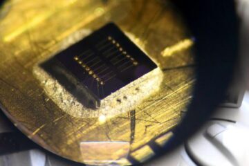
Software corrects chip errors early
Microchip miniaturization is making quality control-related measurement of features during the production process increasingly difficult. New National Institute of Standards and Technology (NIST) software and research results* should help manufacturers reduce errors in measuring microchip features which today measure less than 37 nanometers (about 1.5 millionths of an inch) in width and are expected to shrink to 25 nanometers (about 1 millionth of an inch) by 2007.
Currently, most semiconductor manufacturers use scanning electron microscopes (SEMs) to measure circuitry lines when the chip is first being patterned. Circuit dimensions are formed when ultraviolet light is shined on a thin film of polymer laid over silicon. Exposed areas harden, allowing unexposed areas to be chemically etched into tiny troughs for laying down circuit lines. Errors caught before etching may be correctable, while those caught later may result in scrapping the wafer and loss of a sizeable investment.
The NIST software equips the SEMs with a “model library” of possible line measurements. Technicians can use the enhanced SEMs to match measured images with library images in order to more accurately determine the shapes and sizes of features. Using the new software can cut measurement errors from tens of nanometers down to a few nanometers. The new method also is more reliable. There is about three times less variation among repeated measurements of the same circuit feature using the software than with the current most commonly used method.
NIST and International SEMATECH, a consortium of leading semiconductor manufacturers that represent about half the world’s semiconductor production, funded the “model library” work.
Media Contact
More Information:
http://www.nist.gov/All latest news from the category: Information Technology
Here you can find a summary of innovations in the fields of information and data processing and up-to-date developments on IT equipment and hardware.
This area covers topics such as IT services, IT architectures, IT management and telecommunications.


Newest articles

Sea slugs inspire highly stretchable biomedical sensor
USC Viterbi School of Engineering researcher Hangbo Zhao presents findings on highly stretchable and customizable microneedles for application in fields including neuroscience, tissue engineering, and wearable bioelectronics. The revolution in…

Twisting and binding matter waves with photons in a cavity
Precisely measuring the energy states of individual atoms has been a historical challenge for physicists due to atomic recoil. When an atom interacts with a photon, the atom “recoils” in…
Nanotubes, nanoparticles, and antibodies detect tiny amounts of fentanyl
New sensor is six orders of magnitude more sensitive than the next best thing. A research team at Pitt led by Alexander Star, a chemistry professor in the Kenneth P. Dietrich…

