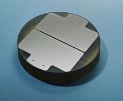
Flat fixtures for EUV exposure
Smaller, even smaller, tiny. Miniaturization in chip manufacture is progressing at an impressive pace. Researchers continue to push the physical limits of semiconductor technology and are developing methods of making circuit elements even smaller and faster. At the same time, the associated processes are having to meet increasingly high requirements.
The experts predict a promising future for EUV lithography – lithography with extremely shortwave ultraviolet light. This works as follows: Light with a wavelength of 13 nanometers is guided through a reflection mask onto the silicon wafers, where it generates nanometer structures.
As the exposure processes take place in a vacuum, special fixtures are necessary to accommodate the silicon wafers and the exposure mask, and to hold them firmly in place. The technical term for these is chucks. Researchers at the Fraunhofer Institute for Applied Optics and Precision Engineering IOF have developed exceptionally precise electrostatic chucks for EUV lithography.
“The chucks need to be extremely smooth and even,” says Fraunhofer IOF scientist Dr. Gerhard Kalkowski. “If they are not super-flat, the result is height deviations in the mask, which lead to structural distortions on the silicon chips.” The IOF researchers are using special glass materials and have developed new technologies to increase the levelness of the chucks, with excellent results: While height deviations of over 100 nanometers had been measured previously, the new material reduced them to 74 nanometers, setting a new record. The chuck and the mask virtually merge into a single plane.
The IOF chucks also have other advantages: “The material guarantees high holding strengths, distributed across the entire surface, and reduces abrasion,” says Kalkowski. Two properties of great importance to the EUV exposure process.
The researchers’ findings will greatly benefit the chip industry, as chip manufacturers rely particularly on the stability and precision of the chucks in order to be able to use EUV lithography in mass production. Meanwhile, the IOF researchers are working towards their next goal: flatter than 50 nanometers.
Media Contact
All latest news from the category: Information Technology
Here you can find a summary of innovations in the fields of information and data processing and up-to-date developments on IT equipment and hardware.
This area covers topics such as IT services, IT architectures, IT management and telecommunications.


Newest articles

Sea slugs inspire highly stretchable biomedical sensor
USC Viterbi School of Engineering researcher Hangbo Zhao presents findings on highly stretchable and customizable microneedles for application in fields including neuroscience, tissue engineering, and wearable bioelectronics. The revolution in…

Twisting and binding matter waves with photons in a cavity
Precisely measuring the energy states of individual atoms has been a historical challenge for physicists due to atomic recoil. When an atom interacts with a photon, the atom “recoils” in…
Nanotubes, nanoparticles, and antibodies detect tiny amounts of fentanyl
New sensor is six orders of magnitude more sensitive than the next best thing. A research team at Pitt led by Alexander Star, a chemistry professor in the Kenneth P. Dietrich…

