Revolutionary Electrode Formation Method for Si Nano Devices Realized by University-IAI Collaboration

The Advanced Electronic Materials Center (Managing Director: Toyohiro Chikyo) of the National Institute for Materials Science (President: Sukekatsu Ushioda), in joint work with Chiba University, Tokyo Institute of Technology, Nagoya University, the University of Tsukuba, Waseda University, and JST-CREST, developed a new electrode formation method for realization of future nano devices.
In this development project, the possibility of controlling the height of the Schottky barrier at metal/Si interfaces by doping only the metal side, without modifying the Si side, was predicted theoretically by Chiba University, and this was demonstrated in collaborative experiments by NIMS, Tokyo Institute of Technology, Nagoya University, the University of Tsukuba, Waseda University, and JST-CREST. This is an unprecedented new electrode formation method.
With Si semiconductors, a good metal/Si bond had been realized by doping the Si side in order to achieve an electrode/Si bond with a low contact resistance value.
However, with miniaturization of devices, deviations in the positions and the concentration of dopants added to the Si side began to affect the metal/Si interface, and it had become impossible to realize a stable electrode structure.
Subsequently, with further miniaturization of the junction region in Si devices, there was a tendency in structural design toward 3-dimensional devices using Si wiring. However, until now, there was no method of forming stable electrodes, and various problems also arose, such as large contact resistance, etc. The results of this research provide a revolutionary method which solves the problems encountered to date.
In integrated circuits and future nano devices, an understanding of the formation process of materials in nano spaces and the properties of those materials from the fundamental mechanism will contribute to solving essential problems. The results of the present research were demonstrated for the first time through collaboration by a large number of research institutions and researchers with various specialties.
Contact information:
For more detail:
Toyohiro Chikyo
Advanced Electronic Materials Center
National Institute for Materials Science
TEL: +81-29-860-4725
E-MailFchikyo.toyohiro@nims.go.jp
For general inquiry:
Public Relations Office, NIMS
TEL:+81-29-859-2026
FAX:+81-29-859-2017
E-MailFpr@nims.go.jp
Media Contact
More Information:
http://www.nims.go.jpAll latest news from the category: Materials Sciences
Materials management deals with the research, development, manufacturing and processing of raw and industrial materials. Key aspects here are biological and medical issues, which play an increasingly important role in this field.
innovations-report offers in-depth articles related to the development and application of materials and the structure and properties of new materials.
Newest articles
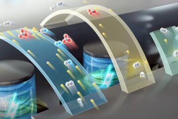
High-energy-density aqueous battery based on halogen multi-electron transfer
Traditional non-aqueous lithium-ion batteries have a high energy density, but their safety is compromised due to the flammable organic electrolytes they utilize. Aqueous batteries use water as the solvent for…

First-ever combined heart pump and pig kidney transplant
…gives new hope to patient with terminal illness. Surgeons at NYU Langone Health performed the first-ever combined mechanical heart pump and gene-edited pig kidney transplant surgery in a 54-year-old woman…
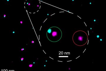
Biophysics: Testing how well biomarkers work
LMU researchers have developed a method to determine how reliably target proteins can be labeled using super-resolution fluorescence microscopy. Modern microscopy techniques make it possible to examine the inner workings…


