Nanowire-bridging transistors open way to next-generation electronics
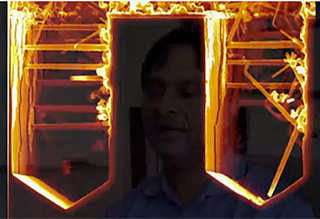
Nanowires grown on Silicon Video (1 min 21 sec) Videography by Andy Fell/UC Davis
Engineers at the University of California, Davis, have recently demonstrated three-dimensional nanowire transistors using this approach that open exciting opportunities for integrating other semiconductors, such as gallium nitride, on silicon substrates.
“Silicon can't do everything,” said Saif Islam, professor of electrical and computer engineering at UC Davis. Circuits built on conventionally etched silicon have reached their lower size limit, which restricts operation speed and integration density. Additionally, conventional silicon circuits cannot function at temperatures above 250 degrees Celsius (about 480 degrees Fahrenheit), or handle high power or voltages, or optical applications.
The new technology could be used, for example, to build sensors that can operate under high temperatures, for example inside aircraft engines.
“In the foreseeable future, society will be dependent on a variety of sensors and control systems that operate in extreme environments, such as motor vehicles, boats, airplanes, terrestrial oil and ore extraction, rockets, spacecraft, and bodily implants,” Islam said.
Devices that include both silicon and nonsilicon materials offer higher speeds and more robust performance. Conventional microcircuits are formed from etched layers of silicon and insulators, but it's difficult to grow nonsilicon materials as layers over silicon because of incompatibilities in crystal structure (or “lattice mismatch”) and differences in thermal properties.
Instead, Islam's laboratory at UC Davis has created silicon wafers with “nanopillars” of materials such as gallium arsenide, gallium nitride or indium phosphide on them, and grown tiny nanowire “bridges” between nanopillars.
“We can't grow films of these other materials on silicon, but we can grow them as nanowires,” Islam said.
The researchers have been able to make these nanowires operate as transistors, and combine them into more complex circuits as well as devices that are responsive to light. They have developed techniques to control the number of nanowires, their physical characteristics and consistency.
Islam said the suspended structures have other advantages: They are easier to cool and handle thermal expansion better than planar structures — a relevant issue when mismatched materials are combined in a transistor.
The technology also leverages the well-established technology for manufacturing silicon integrated circuits, instead of having to create an entirely new route for manufacturing and distribution, Islam said.
The work is described in a series of recent papers in the journals Advanced Materials, Applied Physics Letters and IEEE Transactions on Nanotechnology with co-authors Jin Yong Oh at UC Davis; Jong-Tae Park, University of Incheon, South Korea; Hyun-June Jang and Won-Ju Cho, Kwangwoon University, South Korea. Funding was provided by the U.S. National Science Foundation and the government of South Korea.
UC Davis is a global community of individuals united to better humanity and our natural world while seeking solutions to some of our most pressing challenges. Located near the California state capital, UC Davis has more than 34,000 students, and the full-time equivalent of 4,100 faculty and other academics and 17,400 staff. The campus has an annual research budget of over $750 million, a comprehensive health system and about two dozen specialized research centers. The university offers interdisciplinary graduate study and 99 undergraduate majors in four colleges and six professional schools.
- Saif Islam, Electrical and Computer Engineering, (530) 754-6732, sislam@ucdavis.edu
- Andy Fell, UC Davis News Service, (530) 752-4533, ahfell@ucdavis.edu
Media Contact
More Information:
http://news.ucdavis.edu/search/news_detail.lasso?id=10929All latest news from the category: Materials Sciences
Materials management deals with the research, development, manufacturing and processing of raw and industrial materials. Key aspects here are biological and medical issues, which play an increasingly important role in this field.
innovations-report offers in-depth articles related to the development and application of materials and the structure and properties of new materials.


Newest articles

A universal framework for spatial biology
SpatialData is a freely accessible tool to unify and integrate data from different omics technologies accounting for spatial information, which can provide holistic insights into health and disease. Biological processes…

How complex biological processes arise
A $20 million grant from the U.S. National Science Foundation (NSF) will support the establishment and operation of the National Synthesis Center for Emergence in the Molecular and Cellular Sciences (NCEMS) at…

Airborne single-photon lidar system achieves high-resolution 3D imaging
Compact, low-power system opens doors for photon-efficient drone and satellite-based environmental monitoring and mapping. Researchers have developed a compact and lightweight single-photon airborne lidar system that can acquire high-resolution 3D…

