Major leap towards graphene for solar cells
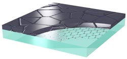
Graphene was deposited onto a glass substrate. The ultrathin layer is but one atomic layer thick (0.3 Angström, or 0.03 nanometers), although charge carriers are able to move about freely within this layer. This property is retained even if the graphene layer is covered with amorphous or polycrystalline silicon.<br><br>Credit: Marc A. Gluba/HZB<br>
Graphene has extreme conductivity and is completely transparent while being inexpensive and nontoxic. This makes it a perfect candidate material for transparent contact layers for use in solar cells to conduct electricity without reducing the amount of incoming light – at least in theory.
Whether or not this holds true in a real world setting is questionable as there is no such thing as “ideal” graphene – a free floating, flat honeycomb structure consisting of a single layer of carbon atoms: interactions with adjacent layers can change graphene's properties dramatically.
“We examined how graphene's conductive properties change if it is incorporated into a stack of layers similar to a silicon based thin film solar cell and were surprised to find that these properties actually change very little,” Marc Gluba explains. To this end, they grew graphene on a thin copper sheet, next transferred it to a glass substrate, and finally coated it with a thin film of silicon. They examined two different versions that are commonly used in conventional silicon thin-film technologies:
one sample contained an amorphous silicon layer, in which the silicon atoms are in a disordered state similar to a hardened molten glas; the other sample contained poly-crystalline silicon to help them observe the effects of a standard crystallization process on graphene's properties.
Even though the morphology of the top layer changed completely as a result of being heated to a temperature of several hundred degrees C, the graphene is still detectable. “That's something we didn't expect to find, but our results demonstrate that graphene remains graphene even if it is coated with silicon,” says Norbert Nickel.
Their measurements of carrier mobility using the Hall-effect showed that the mobility of charge carriers within the embedded graphene layer is roughly 30 times greater than that of conventional zinc oxide based contact layers. Says Gluba: “Admittedly, it's been a real challenge connecting this thin contact layer, which is but one atomic layer thick, to external contacts. We're still having to work on that.” Adds Nickel: “Our thin film technology colleagues are already pricking up their ears and wanting to incorporate it.” The researchers obtained their measurements on one square centimeter samples, although in practice it is feasible to coat much larger areas than that with graphene.
This work was recently published in Applied Physics Letters Vol. 103, 073102 (2013).
Authors: M. A. Gluba, D. Amkreutz, G. V. Troppenz, J. Rappich, and N. H. Nickel
doi: 10.1063/1.4818461
Media Contact
More Information:
http://www.helmholtz-berlin.deAll latest news from the category: Materials Sciences
Materials management deals with the research, development, manufacturing and processing of raw and industrial materials. Key aspects here are biological and medical issues, which play an increasingly important role in this field.
innovations-report offers in-depth articles related to the development and application of materials and the structure and properties of new materials.


Newest articles

A universal framework for spatial biology
SpatialData is a freely accessible tool to unify and integrate data from different omics technologies accounting for spatial information, which can provide holistic insights into health and disease. Biological processes…

How complex biological processes arise
A $20 million grant from the U.S. National Science Foundation (NSF) will support the establishment and operation of the National Synthesis Center for Emergence in the Molecular and Cellular Sciences (NCEMS) at…

Airborne single-photon lidar system achieves high-resolution 3D imaging
Compact, low-power system opens doors for photon-efficient drone and satellite-based environmental monitoring and mapping. Researchers have developed a compact and lightweight single-photon airborne lidar system that can acquire high-resolution 3D…

