Microscopy technique could help computer industry develop 3-D components
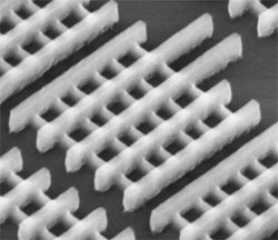
The three-dimensional tri-gate (FinFET) transistors shown here are among the 3-D microchip structures that could be measured using NIST's technique for improving through-focus scanning optical microscopy (TSOM).<br><br>Credit: Courtesy of Intel Corp.<br>
The technique, called Through-Focus Scanning Optical Microscopy (TSOM), has now been shown able to detect tiny differences in the three-dimensional shapes of circuit components, which until very recently have been essentially two-dimensional objects.
TSOM is sensitive to features that are as small as 10 nanometers (nm) across, perhaps smaller—addressing some important industry measurement challenges for the near future for manufacturing process control and helping maintain the viability of optical microscopy in electronics manufacturing.
For decades, computer chips have resembled city maps in which components are essentially flat. But as designers strive to pack more components onto chips, they have reached the same conclusion as city planners: The only direction left to build is upwards. New generations of chips feature 3-D structures that stack components atop one another, but ensuring these components are all made to the right shapes and sizes requires a whole new dimension—literally—of measurement capability.
“Previously, all we needed to do was show we could accurately measure the width of a line a certain number of nanometers across,” explains NIST's Ravikiran Attota. “Now, we will need to measure all sides of a three-dimensional structure that has more nooks and crannies than many modern buildings. And the nature of light makes that difficult.”
Part of the trouble is that components now are growing so small that a light beam can't quite get at them. Optical microscopes are normally limited to features larger than about half the wavelength of the light used—about 250 nanometers for green light. So microscopists have worked around the issue by lining up a bunch of identical components at regular distances apart and observing how light scatters off the group and fitting the data with optical models to determine the dimensions. But these optical measurements, as currently used in manufacturing, have great difficulty measuring newer 3-D structures.
Other non-optical methods of imaging such as scanning probe microscopy are expensive and slow, so the NIST team decided to test the abilities of TSOM, a technique that Attota played a major role in developing. The method uses a conventional optical microscope, but rather than taking a single image, it collects 2-D images at different focal positions forming a 3-D data space. A computer then extracts brightness profiles from these multiple out-of-focus images and uses the differences between them to construct the TSOM image. The TSOM images it provides are somewhat abstract, but the differences between them are still clear enough to infer minute shape differences in the measured structures—bypassing the use of optical models, which introduce complexities that industry must face.
“Our simulation studies show that TSOM might measure features as small as 10 nm or smaller, which would be enough for the semiconductor industry for another decade,” Attota says. “And we can look at anything with TSOM, not just circuits. It could become useful to any field where 3-D shape analysis of tiny objects is needed.”
*R. Attota, B. Bunday and V. Vartanian. Critical dimension metrology by through-focus scanning optical microscopy beyond the 22 nm node. Applied Physics Letters, DOI: 10.1063/1.4809512, published online June 6, 2013.
Media Contact
More Information:
http://www.nist.govAll latest news from the category: Physics and Astronomy
This area deals with the fundamental laws and building blocks of nature and how they interact, the properties and the behavior of matter, and research into space and time and their structures.
innovations-report provides in-depth reports and articles on subjects such as astrophysics, laser technologies, nuclear, quantum, particle and solid-state physics, nanotechnologies, planetary research and findings (Mars, Venus) and developments related to the Hubble Telescope.


Newest articles

High-energy-density aqueous battery based on halogen multi-electron transfer
Traditional non-aqueous lithium-ion batteries have a high energy density, but their safety is compromised due to the flammable organic electrolytes they utilize. Aqueous batteries use water as the solvent for…

First-ever combined heart pump and pig kidney transplant
…gives new hope to patient with terminal illness. Surgeons at NYU Langone Health performed the first-ever combined mechanical heart pump and gene-edited pig kidney transplant surgery in a 54-year-old woman…

Biophysics: Testing how well biomarkers work
LMU researchers have developed a method to determine how reliably target proteins can be labeled using super-resolution fluorescence microscopy. Modern microscopy techniques make it possible to examine the inner workings…

