Thin metasurfaces instead of thick lenses
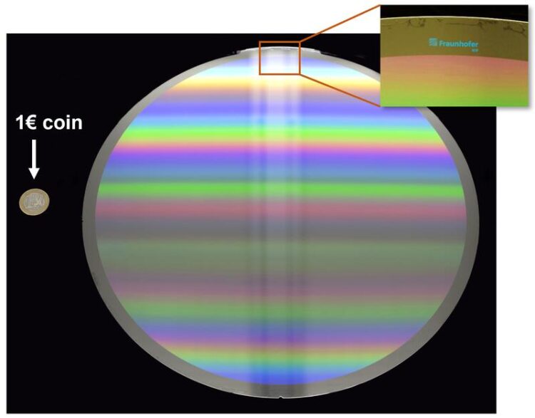
Researchers at Fraunhofer IOF have succeeded for the first time in realizing a metasurface with a diameter of 30 centimeters - here in comparison with a one-euro coin.
© Fraunhofer IOF
Bye bye, lens. Hello metasurface!
So-called metasurfaces can help to make optical systems thinner in the future, while at the same time increasing their functionality. The problem: Until now, conventional manufacturing processes have often only been able to realize small metasurfaces, often smaller than one square millimeter. Researchers at Fraunhofer IOF have now succeeded for the first time in producing a metasurface with a diameter of almost 30 centimeters using electron beam lithography – a world record. The scientists have now published their method in the “Journal of Micro/Nanopatterning, Materials, and Metrology”.
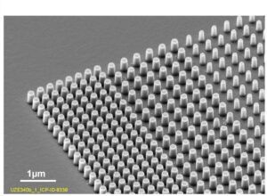
“After 500 years of lenses and mirrors, it is time to think ahead,” explains Dr. Falk Eilenberger, head of the Department of Micro- and Nanostructured Optics at the Fraunhofer Institute for Applied Optics and Precision Engineering IOF. So-called metasurfaces can be an alternative here. These are components that concentrate their complete optical function in a surface and achieve this function in the surface through nanostructures. Eilenberger explains the difference to the classic lens as follows: “In lenses, the function is defined by the macroscopic geometry. That’s why the lens is thick and curved. Now we have a metasurface instead. It’s thin and on scales smaller than the wavelength of light.”
© Fraunhofer IOF
Meta-surfaces have been used in science and research for some time. However, the components here are often only a few square millimeters in size. This is sufficient for academic research, but not for many industrial applications, and certainly not to become a real alternative to the classic lens in the future. Researchers at Fraunhofer IOF in Jena, Germany have therefore devoted themselves to the question of how innovative metasurfaces can be realized on a larger scale. As a result, they are now presenting a metasurface with a diameter of 30 centimeters for the first time. “We are not the inventors of metasurfaces,” Eilenberger holds. “But we are the only ones who can demonstrate it on such a large scale.”
High-resolution structures with high precision and efficiency
But how did the researchers achieve this milestone? The answer: with the help of electron beam lithography. “To produce our metasurface, we used a special writing strategy of electron beam lithography called character projection,” explains Prof. Dr. Uwe Zeitner, a researcher at Fraunhofer IOF and member of the institute’s scientific directorate. Character projection is a method in which a pattern is divided into smaller units. An electron beam is then used to create each of these small patterns in turn on a surface. This enables the fabrication of complex structures with high precision and efficiency. “Using character projection, very high-resolution structures can be exposed in parallel at comparatively high speeds. This is unusual for electron beam lithography,” Zeitner continues. Together with his Fraunhofer colleagues Dr. Michael Banasch and Dr. Marcus Trost, Prof. Zeitner has outlined the potential of electron beam lithography for the fabrication of micro- and nano-optics on large areas in a paper that has now been published in the “Journal of Micro/Nanopatterning, Materials, and Metrology”.
With their paper, the authors show that conventional lithographic techniques often reach their limits for fabricating larger structures. “Due to the small structure dimensions below the wavelength, high-resolution electron beam lithography is in principle very well suited for the fabrication of meta-structures,” the researcher said. “However, this technology is relatively slow. So far essentially only elements with relatively small areas have been realized with it – primarily on the order of a few square millimeters. For larger areas, the exposure time very quickly reaches unrealistically large values.” By using character projection, the scientists were now able to address both the high resolution of electron beam lithography and the large element area without the exposure time “exploding,” according to Uwe Zeitner. The authors of the paper thus show that electron beam lithography can be a technique for fabricating micro- and nano-optical structures on large areas.
Reduction in size with simultaneous increase in functionality
The new manufacturing technology can help build optical systems significantly thinner in the future. “This technology can revolutionize imaging optical systems,” says Falk Eilenberger, for example. “Because it will make it possible to reduce the size of systems while simultaneously increasing their optical functionality.” Uwe Zeitner adds concrete application examples: “Such large metasurfaces are particularly advantageous for compact optics in which large deflection angles are required in a small space. This is the case, for example, in virtual/augmented reality glasses. Advantageous designs can also be realized with such approaches for very small optics in smartphones.” Other potential applications include high-resolution spectroscopy or computer-generated holograms.
Presentation at LASER World of Photonics
The 30-centimeter metasurface will be on public display for the first time at LASER World of Photonics in Munich from June 27 to 30, 2023. The Fraunhofer researchers can be found at booth 415 in hall A2.
Wissenschaftliche Ansprechpartner:
Dr. Falk Eilenberger
Fraunhofer IOF
Head of Department Micro- and Nanostructured Optics
Phone: +49 (0) 3641 807 – 207
Mail: falk.eilenberger@iof.fraunhofer.de
Prof. Dr. Uwe Zeitner
Fraunhofer IOF
Scientific Directorate
Phone: +49 (0) 3641 807 – 403
Mail: uwe.zeitner@iof.fraunhofer.de
Originalpublikation:
Original publication: Uwe D. Zeitner, Michael Banasch, Marcus Trost, “Potential of E-beam lithography for micro- and nano-optics fabrication on large areas,” Journal of Micro/Nanopatterning, Materials, and Metrology, Vol. 22, Issue 4 (June 2023), DOI: 10.1117/1.JMM.22.4.041405, URL: https://caps.luminad.com:8443/stockage/stock/SPIE/LDL-SPIE-JM3-23018SS/JM3-23018….
Weitere Informationen:
https://www.iof.fraunhofer.de/en/pressrelease/2023/metasurface-not-lenses.html
Media Contact
All latest news from the category: Physics and Astronomy
This area deals with the fundamental laws and building blocks of nature and how they interact, the properties and the behavior of matter, and research into space and time and their structures.
innovations-report provides in-depth reports and articles on subjects such as astrophysics, laser technologies, nuclear, quantum, particle and solid-state physics, nanotechnologies, planetary research and findings (Mars, Venus) and developments related to the Hubble Telescope.


Newest articles

Sea slugs inspire highly stretchable biomedical sensor
USC Viterbi School of Engineering researcher Hangbo Zhao presents findings on highly stretchable and customizable microneedles for application in fields including neuroscience, tissue engineering, and wearable bioelectronics. The revolution in…

Twisting and binding matter waves with photons in a cavity
Precisely measuring the energy states of individual atoms has been a historical challenge for physicists due to atomic recoil. When an atom interacts with a photon, the atom “recoils” in…
Nanotubes, nanoparticles, and antibodies detect tiny amounts of fentanyl
New sensor is six orders of magnitude more sensitive than the next best thing. A research team at Pitt led by Alexander Star, a chemistry professor in the Kenneth P. Dietrich…

