New Transistor for Plastic Electronics Exhibits the Best of Both Worlds
Online in the journal Advanced Materials, researchers from the Georgia Institute of Technology describe a new method of combining top-gate organic field-effect transistors with a bilayer gate insulator. This allows the transistor to perform with incredible stability while exhibiting good current performance. In addition, the transistor can be mass produced in a regular atmosphere and can be created using lower temperatures, making it compatible with the plastic devices it will power.
The research team used an existing semiconductor and changed the gate dielectric because transistor performance depends not only on the semiconductor itself, but also on the interface between the semiconductor and the gate dielectric.
“Rather than using a single dielectric material, as many have done in the past, we developed a bilayer gate dielectric,” said Bernard Kippelen, director of the Center for Organic Photonics and Electronics and professor in Georgia Tech’s School of Electrical and Computer Engineering.
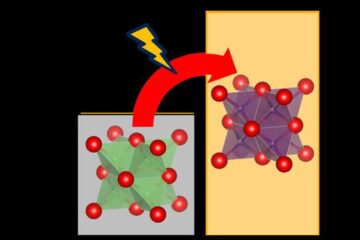
The bilayer dielectric is made of a fluorinated polymer known as CYTOP and a high-k metal-oxide layer created by atomic layer deposition. Used alone, each substance has its benefits and its drawbacks.
CYTOP is known to form few defects at the interface of the organic semiconductor, but it also has a very low dielectric constant, which requires an increase in drive voltage. The high-k metal-oxide uses low voltage, but doesn’t have good stability because of a high number of defects on the interface.
So, Kippelen and his team wondered what would happen if they combined the two substances in a bilayer. Would the drawbacks cancel each other out?
“When we started to do the test experiments, the results were stunning. We were expecting good stability, but not to the point of having no degradation in mobility for more than a year,” said Kippelen.
The team performed a battery of tests to see just how stable the bilayer was. They cycled the transistors 20,000 times. There was no degradation. They tested it under a continuous bias stress where they ran the highest possible current through it. There was no degradation. They even stuck it in a plasma chamber for five minutes. There was still no degradation.
The only time they saw any degradation was when they dropped it into acetone for an hour. There was some degradation, but the transistor was still operational.
No one was more surprised than Kippelen.
“I had always questioned the concept of having air-stable field-effect transistors, because I thought you would always have to combine the transistors with some barrier coating to protect them from oxygen and moisture. We’ve proven ourselves wrong through this work,” said Kippelen.
“By having the bilayer gate insulator we have two different degradation mechanisms that happen at the same time, but the effects are such that they compensate for one another,” explains Kippelen. “So if you use one it leads to a decrease of the current, if you use the other it leads to a shift of the thereshold voltage and over time to an increase of the current. But if you combine them, their effects cancel out.”
“This is an elegant way of solving the problem. So, rather than trying to remove each effect, we took two processes that complement one another and as a result you have a transistor that’s rock stable.”
The transistor conducts current and runs at a voltage comparable to amorphous silicon, the current industry standard used on glass substrates, but can be manufactured at temperatures below 150°C, in line with the capabilities of plastic substrates. It can also be created in a regular atmosphere, making it easier to fabricate than other transistors.
Applications for these transistors include smart bandages, RFID tags, plastic solar cells, light emitters for smart cards – virtually any application where stable power and a flexible surface are needed.
In this paper the tests were performed on glass substrates. Next, the team plans on demonstrating the transistors on flexible plastic substrates. Then they will test the ability to manufacture the bilayer transistors with ink jet printing technologies.
Kippelen’s research team was comprised of Do Kyung Hwang, Canek Fuentes-Hernandez, Jungbae Kim, William J. Postcavage Jr. and Sung-Jin Kim.
The research was supported by Solvay, the Office of Naval Research and the National Science Foundation.
Media Contact
More Information:
http://www.gatech.eduAll latest news from the category: Materials Sciences
Materials management deals with the research, development, manufacturing and processing of raw and industrial materials. Key aspects here are biological and medical issues, which play an increasingly important role in this field.
innovations-report offers in-depth articles related to the development and application of materials and the structure and properties of new materials.


Newest articles

Webb captures top of iconic horsehead nebula in unprecedented detail
NASA’s James Webb Space Telescope has captured the sharpest infrared images to date of a zoomed-in portion of one of the most distinctive objects in our skies, the Horsehead Nebula….
Cost-effective, high-capacity, and cyclable lithium-ion battery cathodes
Charge-recharge cycling of lithium-superrich iron oxide, a cost-effective and high-capacity cathode for new-generation lithium-ion batteries, can be greatly improved by doping with readily available mineral elements. The energy capacity and…

Novel genetic plant regeneration approach
…without the application of phytohormones. Researchers develop a novel plant regeneration approach by modulating the expression of genes that control plant cell differentiation. For ages now, plants have been the…

