Miniaturization of a thermoelectric device capable of powering IoT products
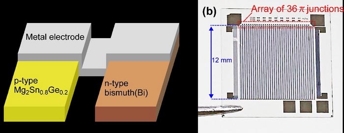
Figure. (a) Enlarged view of a π junction composed of two types of thermoelectric layers connected by a metal electrode. (b) Photo of the thermoelectric device consisting of an array of π junctions.
Credit: National Institute for Materials Science Isao Ohkubo OHKUBO.Isao@nims.go.jp
Semiconductor microfabrication technology enables voltage output greater than 0.5 V.
Using a semiconductor microfabrication technology, a research team consisting of NIMS, AIST and the University of Tsukuba has succeeded in developing a thermoelectric device consisting of an array of π junctions, each composed of two types of thermoelectric layers connected by a metal electrode layer (figure (a)). This device demonstrated the ability to generate voltages greater than 0.5 V, meeting a criterion for certain IoT (internet of things) device operations.
Thermoelectric conversion modules designed to IoT and other electronic devices need to be integrated into these devices. Most previously developed versions of these modules were made of bulk materials, which are incompatible with miniaturization and integration. The output voltages of thermoelectric conversion modules and devices generally decrease as their sizes diminish. An approach to overcoming this miniaturization-related issue is to create an array of π junctions in a thermoelectric device. This research team created a thermoelectric device using a semiconductor microfabrication technology which can be used to produce micro-scale π junctions with a high degree of precision.
This research team fabricated an in-plane thermoelectric device (figure (b)) consisting of a dense array of π junctions, each composed of a p-type Mg2Sn0.8Ge0.2 thin film with high thermoelectric generation efficiency and low electrical resistance, an n-type bismuth layer, which can be produced at room temperature. Despite its small size, this device, equipped with an array of 36 tiny π junctions, was able to generate voltages greater than 0.5 V, satisfying a criterion for certain IoT device operations.
The technique used in this research to create smaller, more compact thermoelectric devices may be used to develop new IoT and other electronic products integrated with thermoelectric devices.
This research was supported by the JST-Mirai project entitled “Utilizing magnetism to develop high-performance thermoelectric materials and devices” (project leader: Takao Mori, project number: JPMJMI19A1).
This research was published in Materials Today Energy, an online journal, on June 18, 2022 (URL: https://doi.org/10.1016/j.mtener.2022.101075). A photo from this publication was used in the figure above with some modifications.
Journal: Materials Today Energy
DOI: 10.1016/j.mtener.2022.101075
Method of Research: Experimental study
Subject of Research: Not applicable
Article Title: Miniaturized in-plane π-type thermoelectric device composed of a II–IV semiconductor thin film prepared by microfabrication
Article Publication Date: 18-Jun-2022
All latest news from the category: Materials Sciences
Materials management deals with the research, development, manufacturing and processing of raw and industrial materials. Key aspects here are biological and medical issues, which play an increasingly important role in this field.
innovations-report offers in-depth articles related to the development and application of materials and the structure and properties of new materials.


Newest articles
Microscopic basis of a new form of quantum magnetism
Not all magnets are the same. When we think of magnetism, we often think of magnets that stick to a refrigerator’s door. For these types of magnets, the electronic interactions…

An epigenome editing toolkit to dissect the mechanisms of gene regulation
A study from the Hackett group at EMBL Rome led to the development of a powerful epigenetic editing technology, which unlocks the ability to precisely program chromatin modifications. Understanding how…

NASA selects UF mission to better track the Earth’s water and ice
NASA has selected a team of University of Florida aerospace engineers to pursue a groundbreaking $12 million mission aimed at improving the way we track changes in Earth’s structures, such…

