Large-area periodic perovskite nanostructures for lenticular printing laser displays

Green- and red-light emission observed at high and low view angles from the periodic nanostructures of mixed-halide perovskite CH3NH3PbBrxI3-x.
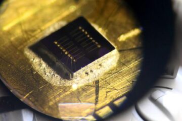
Credit: @Science China Press
Lead halide perovskites, with high refractive index and excellent optoelectronic property, have been used in both constructing high-quality optical resonators/lasers and fabricating high-efficiency light-emitting devices for advanced displays. Lenticular printing provides an illusion of depth and shows varying images upon view angles, which is considered as a promising approach towards future stereoscopic displays.
To realize lenticular-printing-based display, it is required to modulate the outcoupling direction of emission light rather than that of incident light. Ideally, the lenticular-lens-like structures would be integrated into the active layer of light-emitting devices. Therefore, the hybrid perovskite becomes a promising candidate for the investigation of lenticular printing display; however, it remains a challenge to realize large-area periodic structures of perovskite materials especially with a feature size of wavelength scale.
Very recently, Dr. Chuang Zhang, Dr. Yong Sheng Zhao from Institute of Chemistry, Chinese Academy of Sciences, Dr. Yuchen Wu from Technical Institute of Physics and Chemistry, Chinese Academy of Sciences, and their colleagues fabricated lead halide perovskite periodic structures via a space-confined solution growth method.
The spatial resolution could be down to hundreds of nanometers while the substrate size up to several centimeters. These structures were able to not only modulate the reflection of visible light, but also control the angle of light emission from hybrid perovskites. More importantly, the low-threshold lasing based on distributed feedback was observed from the periodic structures, and its narrow line-width offered possibility to realize the lenticular printing laser display, according to the wavelength-dependent outcoupling of emission colors.
A prototype of laser display panels was then realized based on the mixed halide perovskites, in which the green and red colored images were obtained at high and low angles respectively. This work would shed light on the design and fabrication of perovskites materials for new types of display techniques.
###
See the article: Wang M, Li H, Dai C, Tang J, Yin B, Wang H, Li J, Wu Y, Zhang C, Zhao YS. Large-area periodic lead halide perovskite nanostructures for lenticular printing laser displays. Sci. China Chem., 2020, DOI: 10.1007/s11426-020-9919-6.
https:/
All latest news from the category: Materials Sciences
Materials management deals with the research, development, manufacturing and processing of raw and industrial materials. Key aspects here are biological and medical issues, which play an increasingly important role in this field.
innovations-report offers in-depth articles related to the development and application of materials and the structure and properties of new materials.


Newest articles

Sea slugs inspire highly stretchable biomedical sensor
USC Viterbi School of Engineering researcher Hangbo Zhao presents findings on highly stretchable and customizable microneedles for application in fields including neuroscience, tissue engineering, and wearable bioelectronics. The revolution in…

Twisting and binding matter waves with photons in a cavity
Precisely measuring the energy states of individual atoms has been a historical challenge for physicists due to atomic recoil. When an atom interacts with a photon, the atom “recoils” in…
Nanotubes, nanoparticles, and antibodies detect tiny amounts of fentanyl
New sensor is six orders of magnitude more sensitive than the next best thing. A research team at Pitt led by Alexander Star, a chemistry professor in the Kenneth P. Dietrich…

