Cracking a Tough Nut for the Semiconductor Industry
The new technique could help improve the reliability and manufacturability of ICs and, better yet, it’s one that state-of-the-art microelectronics manufacturers can use with equipment they already own.
At issue is the mechanical strength of so-called “low-k” dielectric layers—electrically insulating films only a couple of micrometers thick that are interleaved between layers of conductors and components in microprocessor chips and other high-performance semiconductor devices. As IC features like transistors have gotten ever smaller and crammed more closely together, designers are preventing electrical interference or “cross-talk” by making the insulating films more and more porous with nanoscale voids—but this has made them more fragile. Brittle fracture failure of low-k insulating films remains a problem for the industry, affecting both manufacturing yields and device reliability. To date, there has been no accurate method to measure the fracture resistance of such films, which makes it difficult to design improved dielectrics.
NIST researchers believe they have found an answer to the measurement problem in a new adaptation of a materials test technique called nanoindentation. Nanoindentation works by pressing a sharp, hard object—a diamond tip—and observing how much pressure it takes to deform the material. For roughly 20 years, researchers have known how to measure elasticity and plasticity—the forces needed to bend a material either temporarily or permanently—of materials at very small scales with nanoindenters. But toughness, the force needed to actually break the material, has been, well, tougher. Thin films were particularly problematic because they necessarily must be layered on top of another stronger material, such as a silicon wafer.
The new NIST technique requires a slight modification of the nanoindentation equipment—the probe has to have a sharper, more acute point than normally used—and a hefty dose of theory. Pressing carefully on the dielectric film generates cracks as small as 300 nanometers, which are measured by electron microscopy. Just how the cracks form depends on a complex interaction involving indentation force, film thickness, film stress and the elastic properties of the film and the silicon substrate. These variables are plugged into a new fracture mechanics model that predicts not only the fracture toughness but also another key value, the critical film thickness for spontaneous fracture.
Using this methodology, device manufacturers will be able to eliminate some candidate interconnect dielectric films from consideration without further expensive device testing. The measurement technique and model were published in a two-part series in the Journal of Materials Research.*
* D.J. Morris and R.F. Cook. Indentation fracture of low-dielectric constant films: Part I. Experiments and observations. J. Mater. Res., Vol. 23, No. 9, p. 2429.
* D.J. Morris and R.F. Cook. Indentation fracture of low-dielectric constant films: Part II. Indentation fracture mechanics model. J. Mater. Res., Vol. 23, No. 9, p. 2443.
Media Contact
More Information:
http://www.nist.govAll latest news from the category: Materials Sciences
Materials management deals with the research, development, manufacturing and processing of raw and industrial materials. Key aspects here are biological and medical issues, which play an increasingly important role in this field.
innovations-report offers in-depth articles related to the development and application of materials and the structure and properties of new materials.


Newest articles
Recovering phosphorus from sewage sludge ash
Chemical and heat treatment of sewage sludge can recover phosphorus in a process that could help address the problem of diminishing supplies of phosphorus ores. Valuable supplies of phosphorus could…
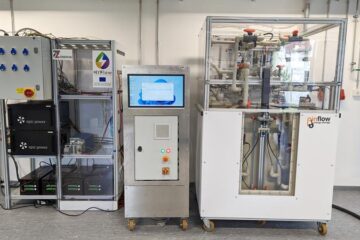
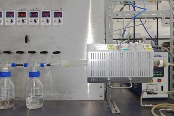
Efficient, sustainable and cost-effective hybrid energy storage system for modern power grids
EU project HyFlow: Over three years of research, the consortium of the EU project HyFlow has successfully developed a highly efficient, sustainable, and cost-effective hybrid energy storage system (HESS) that…
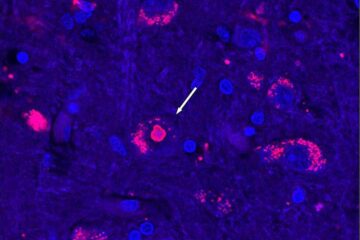
After 25 years, researchers uncover genetic cause of rare neurological disease
Some families call it a trial of faith. Others just call it a curse. The progressive neurological disease known as spinocerebellar ataxia 4 (SCA4) is a rare condition, but its…

