Strong cooperation forges global advances in semiconductor processing
Thanks to a series of highly successful projects in the EUREKA MEDEA+ Cluster, Europe leads the way in extreme ultraviolet (EUV) lithography for the production of future generations of semiconductor chips. As a result of strong co-operation between chipmakers, equipment suppliers and research centres, European companies will dominate the world market for equipment and materials. This is expected to generate some 18,000 jobs, mainly at a high technical level, as well as a €1 billion turnover by 2009.
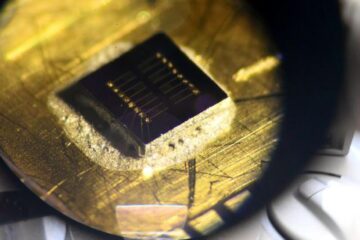
Lithography plays a key role in the production of integrated circuits and now accounts for some 35% of the processing cost of silicon chips. It involves directing light through a photomask to project an image of the desired circuit onto the silicon semiconductor wafer covered with a light-resistant photoresist. As circuit details become smaller and smaller, the wavelength of the light has also reduced and is reaching the limits of the deep ultraviolet range. The solution for future generations of even smaller dimensioned circuits is the use of EUV with a wavelength of 13.5 nm, which are actually considered as soft X-rays.
Covering the main elements of the lithography process
The projects focused on the main elements of the lithography process including tools, masks, illumination sources and processing. Extensive work was carried out on optics and coating technologies for project T403 EXTATIC which has led to the development of a full-field EUV lithographic research tool essential for future research – two tools are being delivered in 2006. Developing a complete mask-making process for 45 nm circuit structures and below was the aim in the T404 EXTUMASK project. First commercial masks have now been delivered to ASML – the Netherlands-based global leader in chipmaking lithography equipment. T405 EUV SOURCES focused on high power sources and achieved world record outputs, meaning power sources are no longer a blocking issue. Finally, the T406 EXITE project set out to eliminate the bottlenecks related to EUV imaging for full-field development.
“The EUV projects are achieving remarkable results and Europe is now at the leading edge of the technology globally,” says Rob Hartman of ASML and chairman of the MEDEA+ EUV Cluster Steering Council (CSC). “It was working in cooperation within the framework of the EUREKA MEDEA+ Cluster that made this success possible.”
Media Contact
More Information:
http://www.eureka.be/inaction/viewSuccessStory.do?docid=1646128All latest news from the category: Information Technology
Here you can find a summary of innovations in the fields of information and data processing and up-to-date developments on IT equipment and hardware.
This area covers topics such as IT services, IT architectures, IT management and telecommunications.


Newest articles

Sea slugs inspire highly stretchable biomedical sensor
USC Viterbi School of Engineering researcher Hangbo Zhao presents findings on highly stretchable and customizable microneedles for application in fields including neuroscience, tissue engineering, and wearable bioelectronics. The revolution in…

Twisting and binding matter waves with photons in a cavity
Precisely measuring the energy states of individual atoms has been a historical challenge for physicists due to atomic recoil. When an atom interacts with a photon, the atom “recoils” in…
Nanotubes, nanoparticles, and antibodies detect tiny amounts of fentanyl
New sensor is six orders of magnitude more sensitive than the next best thing. A research team at Pitt led by Alexander Star, a chemistry professor in the Kenneth P. Dietrich…

