Silicon nanowires upgrade data-storage technology

As reported in a recent paper,* the device is a type of “non-volatile” memory, meaning stored information is not lost when the device is without power. So-called “flash” memory (used in digital camera memory cards, USB memory sticks, etc.) is a well-known example of electronic non-volatile memory. In this new device, nanowires are integrated with a higher-end type of non-volatile memory that is similar to flash, a layered structure known as semiconductor-oxide-nitride-oxide-semiconductor (SONOS) technology. The nanowires are positioned using a hands-off self-alignment technique, which could allow the production cost—and therefore the overall cost—of large-scale viable devices to be lower than flash memory cards, which require more complicated fabrication methods.
The researchers grew the nanowires onto a layered oxide-nitride-oxide substrate. Applying a positive voltage across the wires causes electrons in the wires to tunnel down into the substrate, charging it. A negative voltage causes the electrons to tunnel back up into the wires. This process is the key to the device’s memory function: when fully charged, each nanowire device stores a single bit of information, either a “0” or a “1” depending on the position of the electrons. When no voltage is present, the stored information can be read.
The device combines the excellent electronic properties of nanowires with established technology, and thus has several characteristics that make it very promising for applications in non-volatile memory. For example, it has simple read, write, and erase capabilities. It boasts a large memory window—the voltage range over which it stores information—which indicates good memory retention and a high resistance to disturbances from outside voltages. The device also has a large on/off current ratio, a property that allows the circuit to clearly distinguish between the “0” and “1” states.
Two advantages the NIST design may hold over alternative proposals for nanowire-based memory devices, the researchers say, are better stability at higher temperatures and easier integration into existing chip fabrication technology.
* Q. Li, X. Zhu, H. Xiong, S.-M. Koo, D.E. Ioannou, J. Kopanski, J.S. Suehle and C.A. Richter. Silicon nanowire on oxide/nitride/oxide for memory application. Nanotechnology 18 (2007) 235204.
Media Contact
More Information:
http://www.nist.govAll latest news from the category: Physics and Astronomy
This area deals with the fundamental laws and building blocks of nature and how they interact, the properties and the behavior of matter, and research into space and time and their structures.
innovations-report provides in-depth reports and articles on subjects such as astrophysics, laser technologies, nuclear, quantum, particle and solid-state physics, nanotechnologies, planetary research and findings (Mars, Venus) and developments related to the Hubble Telescope.
Newest articles

A universal framework for spatial biology
SpatialData is a freely accessible tool to unify and integrate data from different omics technologies accounting for spatial information, which can provide holistic insights into health and disease. Biological processes…

How complex biological processes arise
A $20 million grant from the U.S. National Science Foundation (NSF) will support the establishment and operation of the National Synthesis Center for Emergence in the Molecular and Cellular Sciences (NCEMS) at…
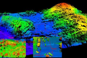
Airborne single-photon lidar system achieves high-resolution 3D imaging
Compact, low-power system opens doors for photon-efficient drone and satellite-based environmental monitoring and mapping. Researchers have developed a compact and lightweight single-photon airborne lidar system that can acquire high-resolution 3D…


