X-rays reveal molecular arrangements for better printable electronics
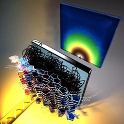
This is an image of a printed electronics system.<br>Credit: Peter Allen<br>
“This work is exciting because it helps reveal in new detail how we can achieve high performance transistors and solar cells with polymers,” said UC Santa Barbara professor of materials Michael Chabinyc, who, with UCSB chemistry graduate student Justin Cochran and North Carolina State physicists Harald Ade and Brian Collins, set out to find out which materials and which processing steps worked better, in what is still a largely trial-and-error process for manufacturers of printable electronics. This effort also involved collaboration with an international team, including researchers from Monash University in Australia and Univeristät Erlangen-Nümberg in Germany.
Printed electronics is a process that employs fairly common printing methods to deposit inks containing organic conductive molecules onto surfaces, to creating circuitry for a variety of electronic devices, including photovoltaics, displays, and even luminescent clothing. The process is faster and cheaper than conventional production techniques for the same products, and could pave the way toward making these devices more accessible to consumers.
However, until recently, the process of selecting these organic materials –– and what steps to take in order to improve their performance –– was something of a mystery. Some materials and treatments worked better than others, and the researchers set out to find out why.
The researchers developed a technique that used powerful X-rays to peer into these organic materials at the molecular level. They found that the performance of the material had to do with its molecular alignment, and that this alignment was controlled by simple methods such as heating and molecular interactions at surface levels.
“In transistors, we found that as the alignment between molecules increased, so did the performance,” Collins said. “In the case of the solar cells, we discovered alignment of molecules at interfaces in the device, which may be the key to more efficient harvesting of light. For both, this was the first time anyone had been able to really look at what was happening at the molecular level.”
The researchers hope that the new X-ray technique will provide a better perspective into the nature of organic materials used in printed electronics.
“We're hoping that this technique will give researchers and manufacturers greater insight into the fundamentals of these materials,” Collins said. “Understanding how these materials work can only lead to improved performance and better commercial viability.”
Funding for work on organic transistors at UCSB and NCSU was supported by the Division of Materials Research of the National Science Foundation, through an award from the American Recovery and Reinvestment Act.
Media Contact
More Information:
http://www.ucsb.eduAll latest news from the category: Materials Sciences
Materials management deals with the research, development, manufacturing and processing of raw and industrial materials. Key aspects here are biological and medical issues, which play an increasingly important role in this field.
innovations-report offers in-depth articles related to the development and application of materials and the structure and properties of new materials.


Newest articles

A universal framework for spatial biology
SpatialData is a freely accessible tool to unify and integrate data from different omics technologies accounting for spatial information, which can provide holistic insights into health and disease. Biological processes…

How complex biological processes arise
A $20 million grant from the U.S. National Science Foundation (NSF) will support the establishment and operation of the National Synthesis Center for Emergence in the Molecular and Cellular Sciences (NCEMS) at…

Airborne single-photon lidar system achieves high-resolution 3D imaging
Compact, low-power system opens doors for photon-efficient drone and satellite-based environmental monitoring and mapping. Researchers have developed a compact and lightweight single-photon airborne lidar system that can acquire high-resolution 3D…

