Novel solid-state nanomaterial platform enables terahertz photonics
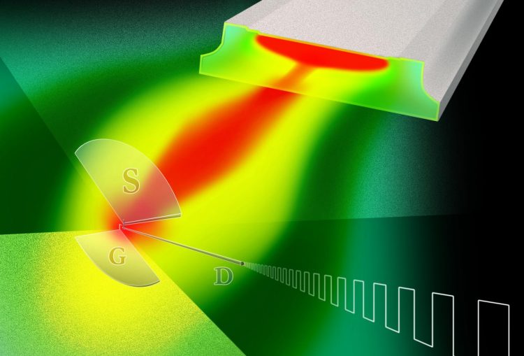
This schematic shows nanowire detectors coupled with THz quantum cascade lasers. Credit: AIP Publishing
Compact, sensitive and fast nanodetectors are considered to be somewhat of a “Holy Grail” sought by many researchers around the world. And now a team of scientists in Italy and France has been inspired by nanomaterials and has created a novel solid-state technology platform that opens the door to the use of terahertz (THz) photonics in a wide range of applications.
During the past decade, materials research has played an essential role in filling the THz gap, beginning with the development of THz quantum cascade lasers, which rely heavily on semiconductor heterostructured artificial nanomaterials. The development of THz spectroscopy, nanospectroscopy and THz imaging expanded the range of powerful tools for the characterization of a broad range of materials — including one-dimensional or two-dimensional semiconductors, biomolecules and graphene.
The missing piece? A complementary detection technology capable of fulfilling THz application-oriented needs in fields such as biomedical diagnostics, security, cultural heritage, quality and process controls, and high data-rate wireless communications that require ad hoc integrated generation and detection systems.
As the scientists report in the journal APL Materials, from AIP publishing, by using an approach that exploits the excitation of plasma waves in the channel of field-effect transistors (FET), they were able to create the first FET detectors based on semiconductor nanowires, designed in a plethora of architectures — including tapers, heterostructures and metamaterial-antenna coupled. While they were at it, they also developed the first THz detectors made of mono- or bi-layer graphene.
“Our work shows that nanowire FET technology is versatile enough to enable 'design' via lithography of the detector's parameters and its main functionalities,” explained Miriam Serena Vitiello, lead author of the paper as well as research scientist and group leader of Terahertz Photonics Group in the Nanoscience Institute at CNR and Scuola Normale Superiore in Pisa, Italy.
What's the nanowire detector capable of? It offers “a concrete perspective of application-oriented use, since it operates at room temperature — reaching detection frequencies greater than 3 THz, with maximum modulation speed in the MHz range, and noise equivalent powers that are already competitive with the best commercially available technologies,” Vitiello said.
In terms of applications, because the nanodetectors can be tapped for large-area fast imaging across both the THz and the sub-terahertz spectral ranges, don't be surprised to see them commercialized in the near future for a variety of spectroscopic and real-time imaging applications — possibly even in the form of fast multi-pixel THz cameras.
Next, the scientists' goals are to “push the device's performance in the ultrafast detection realm, explore the feasibility of single photon detection by using novel architectures and material choices, develop compact focal plane arrays, and to integrate on-chip the nanowire detectors with THz quantum cascade microlasers,” noted Vitiello. “This will allow us to take THz photonics to a whole new level of 'compactness' and versatility, where it can finally begin to address many killer applications.”
The article, “One dimensional semiconductor nanostructures: an effective active-material for TeraHertz detection,” is authored by Miriam S. Vitiello, Leonardo Viti, Dominique Coquillat, Wojciech Knap, Daniele Ercolani and Lucia Sorba. It will appear in the journal APL Materials on February 17, 2015 (DOI: 10.1063/1.4906878). After that date, it can be accessed at: http://scitation.
The authors of this paper are affiliated with CNR Instituto Nanoscienze-NEST, Sculola Normale Superiore, CNRS Université Montpellier 2.
ABOUT THE JOURNAL
APL Materials is a new open access journal featuring original research on significant topical issues within the field of materials science. See: http://aplmaterials.
Media Contact
All latest news from the category: Materials Sciences
Materials management deals with the research, development, manufacturing and processing of raw and industrial materials. Key aspects here are biological and medical issues, which play an increasingly important role in this field.
innovations-report offers in-depth articles related to the development and application of materials and the structure and properties of new materials.


Newest articles

A universal framework for spatial biology
SpatialData is a freely accessible tool to unify and integrate data from different omics technologies accounting for spatial information, which can provide holistic insights into health and disease. Biological processes…

How complex biological processes arise
A $20 million grant from the U.S. National Science Foundation (NSF) will support the establishment and operation of the National Synthesis Center for Emergence in the Molecular and Cellular Sciences (NCEMS) at…

Airborne single-photon lidar system achieves high-resolution 3D imaging
Compact, low-power system opens doors for photon-efficient drone and satellite-based environmental monitoring and mapping. Researchers have developed a compact and lightweight single-photon airborne lidar system that can acquire high-resolution 3D…

