Advanced imaging techniques

Advanced imaging techniques on a semiconductor material reveal ‘surprising’ hidden activity (c) Ella Maru Studio / PDI
…on a semiconductor material reveal ‘surprising’ hidden activity.
New research suggests that materials commonly overlooked in computer chip design actually play an important role in information processing; a discovery that could lead to faster and more efficient electronics. The international team observed surprising activity in a semiconductor material using advanced imaging techniques. The finding could lead to faster and more energy-efficient electronic devices, according to the team from the Pennsylvania State University (USA) and Paul Drude Institute for Solid State Electronics (Berlin, Germany).

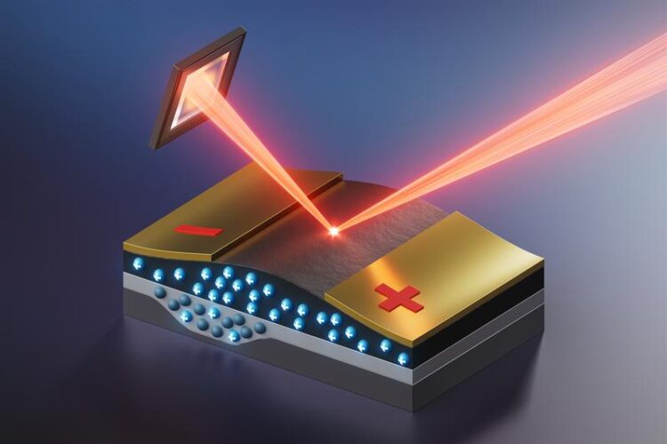
a:Schematic of in-operando synchrotron X-ray setup b:Voltage vs. time of applied pulse & voltage drop across resistor c:Time-resolved shifts in Bragg peak during IMT in x-direction & y–z plane at ≈26° angle d:Lattice distortion schematic across VO2 channel. Credit: Advanced Materials (2024). DOI: 10.1002/adma.202312673
For the first time, a team of researchers has observed a semiconductor material actively flipping behavior from that of an insulator to that of a metal and back in a real device geometry using advanced imaging techniques. This unique imaging of a live fully-functioning electronic device using X-ray “diffraction microscopy” also revealed unexpected activity in the substrate below. The finding could lead to faster and more energy-efficient devices, according to the team from the Pennsylvania State University (USA) and Paul Drude Institute for Solid State Electronics (Berlin, Germany).
The researchers worked with the semiconductor material, vanadium dioxide (VO2), which they said shows great potential as an electronic switch. They also studied how vanadium dioxide interacts with the substrate material titanium dioxide and were surprised to discover that there seems to be an active layer in the substrate that behaves similarly to the semiconductor material on top of it when the semiconductor switches between an insulator (not letting electricity flow) and a metal (letting electricity flow). The revelation that substrates can play an active role in semiconductor processes is significant for designing future materials and devices, said study lead Venkatraman Gopalan, professor of materials science and engineering and of physics at Penn State.
Modern computers have billions of transistors made of semiconductors, and they can be switched between two states — zero and one — by applying a voltage across them. “Smartphones and laptops contain billions of transistors,” said Roman Engel-Herbert, Director of the Paul Drude Institute for Solid State Electronics, and co-author of the study in Advanced Materials. “To process information and perform calculations we have to switch between the two states of the transistor, and each switch requires energy. The sheer volume of transistors in use today is driven by the demand for more data centers, which are the largest and fastest-growing drivers of energy consumption. We need to find materials that can switch between the two transistor states in a much more energy-efficient manner to meet the demand for faster computing devices.”
Gopalan added, “One idea being pursued is materials, such as VO2, that can switch between metal (the one state) and insulator (the zero state) in a trillionth of a second. This is known as undergoing metal-insulator transitions.”
The potential of VO2 as a metal-to-insulator transistor is well-documented and the material is considered promising for semiconductor technology due to its low energy consumption, Gopalan said. However, the material’s properties are still not fully understood, and until now, it has usually been studied in isolation rather than while functioning in a real device.
In addition, VO2 exhibits strong correlated electronic effects, meaning the repulsion between electrons cannot be ignored as is currently done in silicon-based electronics. This characteristic can result in materials with novel functionalities such as high-temperature superconductivity and enhanced magnetic properties.
“The underlying physics of this material is less understood, and its performance in a device geometry is even lesser understood,” Gopalan said. “If we can make them work, there will be a renaissance in electronics. In particular, neuromorphic computing — where computer systems that take inspiration from the brains of living systems with neurons — could seriously benefit by using such devices.”
The team designed an experiment to investigate VO2 in a device geometry rather than in isolation, applying a voltage to make it switch from its insulating to a conducting state. They used powerful X-ray beams at the Advanced Photon Source (APS) at the Argonne National Laboratory to study the structural response of materials on the atomic level with high spatial and temporal resolution. Operating the VO2 device while mapping its spatial and temporal response to the switching event, the researchers observed unexpected changes to the structure of the material and substrate.
“What we found was that as the VO2 film changes to a metal, the whole film channel bulges, which is very surprising,” said Gopalan. “Normally it is supposed to shrink. So clearly something else was going on in the film geometry that was missed before.”
The APS X-ray can penetrate through the VO2 film and also probe the titanium dioxide (TiO2) substrate onto which the VO2 film was grown. The substrate is normally considered an electrically and mechanically passive material.
“We found to our great surprise that this substrate is very much active, jiving and responding in completely surprising ways as the film switches from an insulator to a metal and back when the electrical pulses arrive,” Gopalan said. “This is like watching the tail wagging the dog, which stumped us for a long while. This surprising and previously overlooked observation completely changes how we need to view this technology.”
To understand these findings, the theory and simulation effort — led by Long-Qing Chen, Hamer Professor of Materials Science and Engineering, professor of engineering science and mechanics and of mathematics at Penn State — developed a theoretical framework to explain the entire process of the film and the substrate bulging instead of shrinking. When their model incorporated naturally occurring missing oxygen atoms in this material of two types, charged and uncharged, the experimental results could be satisfactorily explained.
“These neutral oxygen vacancies hold a charge of two electrons, which they can release when the material switches from an insulator to a metal,” Gopalan said. “The oxygen vacancy left behind is now charged and the crystal swells up, leading to the observed surprising bulging in the device. This response can also happen in the substrate. All of these physical processes are beautifully captured in the phase-field theory and modeling performed in this work for the first time by the postdoc Yin Shi in Prof. Chen’s group.”
Gopalan and Engel-Herbert credited the multidisciplinary team’s combined expertise in material growth, synthesis, structure analysis and synchrotron beamline operation with the new understanding. Using a collaborative approach led by Greg Stone, the lead experimental author and Yin Chi, the lead theory author, the researchers disentangled the material’s responses and observed them individually using phase field simulations, a simulation that helps scientists understand material changes over time by depicting various states of matter in a virtual setting.
“By bringing these experts together and pooling our understanding of the problem, we were able to go far beyond our individual scope of expertise and discover something new,” said Engel-Herbert, whose group grew these films along with Darrell Schlom’s group at Cornell. “Recognizing the potential of functional materials necessitates an appreciation of their broader context, just as complex scientific challenges can only be solved through widening our individual perspectives.”
The responses themselves require further investigation, researchers said, but they believe that understanding them will assist in identifying previously unknown capabilities of VO2, including potential yet-to-be-discovered phenomena in the TiO2 substrate that was considered passive before this study. The study itself unfolded over 10 years, Gopalan noted, including validating the results.
“This is what it takes to go from interesting science to a working device you can hold in the palm of your hand,” Gopalan said. “Experiments and theory are complex and require large-scale collaborative teams working closely together over an extended period of time to solve difficult problems that could have a large impact. We hope and expect that this will accelerate the progress towards a new generation of electronic devices.”
Along with Gopalan and Engel-Herbert, other authors of the paper include Yin Shi, a postdoctoral scholar; Matthew Jerry, a graduate student; Vladimir Stoica, A research associate professor; and Long-Qing Chen, A distinguished Professor, all from Penn State; Hanjong Paik and Darrell G. Schlom from Cornell University; Zhonghou Cai and Haidan Wen from the Argonne National Laboratory, and Suman Datta from the Georgia Institute of Technology. The U.S. Department of Energy primarily supported this work. Film growth was supported by the National Science Foundation.
Wissenschaftliche Ansprechpartner:
Venkatraman Gopalan, Department of Materials Science and Engineering, Penn State College of Earth and Mineral Sciences, 221 Steidle Building, University Park, PA 16802, USA
Email: gopalan@matse.psu.edu
Prof. Dr. Roman Engel-Herbert, Paul Drude Institute for Solid State Electronics (PDI)., Hausvogteiplatz 5-7, 10117 Berlin, Germany.
Email: engel-herbert@pdi-berlin.de
Originalpublikation:
Title: In-Operando Spatiotemporal Imaging of Coupled Film-Substrate Elastodynamics during an Insulator-to-Metal Transition
Authors: Greg Stone, Yin Shi, Matthew Jerry, Vladimir Stoica, Hanjong Paik, Zhonghou Cai, Darrell G. Schlom, Roman Engel-Herbert, Suman Datta, Haidan Wen, Long-Qing Chen, and Venkatraman Gopalan
Journal: Advanced Materials
DOI: 10.1002/adma.202312673
https://onlinelibrary.wiley.com/doi/full/10.1002/adma.202312673
Weitere Informationen:
https://www.pdi-berlin.de/news-events/latest-news/semiconductor-material-reveals…
Media Contact
All latest news from the category: Materials Sciences
Materials management deals with the research, development, manufacturing and processing of raw and industrial materials. Key aspects here are biological and medical issues, which play an increasingly important role in this field.
innovations-report offers in-depth articles related to the development and application of materials and the structure and properties of new materials.
Newest articles

A universal framework for spatial biology
SpatialData is a freely accessible tool to unify and integrate data from different omics technologies accounting for spatial information, which can provide holistic insights into health and disease. Biological processes…

How complex biological processes arise
A $20 million grant from the U.S. National Science Foundation (NSF) will support the establishment and operation of the National Synthesis Center for Emergence in the Molecular and Cellular Sciences (NCEMS) at…

Airborne single-photon lidar system achieves high-resolution 3D imaging
Compact, low-power system opens doors for photon-efficient drone and satellite-based environmental monitoring and mapping. Researchers have developed a compact and lightweight single-photon airborne lidar system that can acquire high-resolution 3D…


