Researchers create laser the size of a virus particle
A Northwestern University research team has found a way to manufacture single laser devices that are the size of a virus particle and that operate at room temperature.
These plasmonic nanolasers could be readily integrated into silicon-based photonic devices, all-optical circuits and nanoscale biosensors.
Reducing the size of photonic and electronic elements is critical for ultra-fast data processing and ultra-dense information storage. The miniaturization of a key, workhorse instrument — the laser — is no exception.
The results are published in the journal Nano Letters.
“Coherent light sources at the nanometer scale are important not only for exploring phenomena in small dimensions but also for realizing optical devices with sizes that can beat the diffraction limit of light,” said Teri Odom, a nanotechnology expert who led the research.
Odom is the Board of Lady Managers of the Columbian Exposition Professor of Chemistry in the Weinberg College of Arts and Sciences and a professor of materials science and engineering in the McCormick School of Engineering and Applied Science.
“The reason we can fabricate nano-lasers with sizes smaller than that allowed by diffraction is because we made the lasing cavity out of metal nanoparticle dimers — structures with a 3-D 'bowtie' shape,” Odom said.
These metal nanostructures support localized surface plasmons — collective oscillations of electrons — that have no fundamental size limits when it comes to confining light.
The use of the bowtie geometry has two significant benefits over previous work on plasmon lasers: (1) the bowtie structure provides a well-defined, electromagnetic hot spot in a nano-sized volume because of an antenna effect, and (2) the individual structure has only minimal metal “losses” because of its discrete geometry.
“Surprisingly, we also found that when arranged in an array, the 3-D bowtie resonators could emit light at specific angles according to the lattice parameters,” Odom said.
The Nano Letters paper, titled “Plasmonic Bowtie Nanolaser Arrays,” is available at http://dx.doi.org/10.1021/nl303086r.
Media Contact
More Information:
http://www.northwestern.eduAll latest news from the category: Process Engineering
This special field revolves around processes for modifying material properties (milling, cooling), composition (filtration, distillation) and type (oxidation, hydration).
Valuable information is available on a broad range of technologies including material separation, laser processes, measuring techniques and robot engineering in addition to testing methods and coating and materials analysis processes.


Newest articles
Recovering phosphorus from sewage sludge ash
Chemical and heat treatment of sewage sludge can recover phosphorus in a process that could help address the problem of diminishing supplies of phosphorus ores. Valuable supplies of phosphorus could…
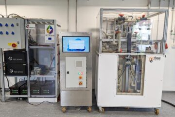
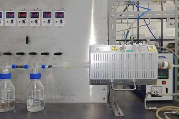
Efficient, sustainable and cost-effective hybrid energy storage system for modern power grids
EU project HyFlow: Over three years of research, the consortium of the EU project HyFlow has successfully developed a highly efficient, sustainable, and cost-effective hybrid energy storage system (HESS) that…

After 25 years, researchers uncover genetic cause of rare neurological disease
Some families call it a trial of faith. Others just call it a curse. The progressive neurological disease known as spinocerebellar ataxia 4 (SCA4) is a rare condition, but its…

