New stamping process creates metallic interconnects, nanostructures
“Solid-state superionic stamping offers a new approach, both as a stand-alone process and as a complement to other nanofabrication techniques, for creating chemical sensors, photonic structures and electrical interconnects,” said Nicholas X. Fang, a professor of mechanical science and engineering, and corresponding author of a paper published in the Feb. 14 issue of the journal Nano Letters.
The S4 process uses a patterned superionic material as a stamp, and etches a metallic film by an electrochemical reaction. In superionic materials, metal ions can move almost freely around the crystal lattice. These mobile materials can also be used in batteries and fuel cells.
Unlike conventional processing – in which patterns are first placed on photoresist, followed by metal deposition and subsequent etching – the S4 process creates high-resolution metallic nanopatterns in a single step, potentially reducing manufacturing costs and increasing yields.
The S4 process begins by carving the desired pattern into a stamp made of superionic material, such as silver sulfide, using focused ion beam milling. The stamp is then placed on the substrate and a voltage is applied. This produces an electrochemical reaction at the contact points of the interface.
The reaction generates metal ions, which migrate across the interface into the stamp. As the reaction continues, the stamp progresses into the substrate, generating features complementary to the pattern on the stamp.
“The stamp acts like a sponge, soaking up metal ions,” said Fang, who also is a researcher at the university's Beckman Institute for Advanced Science and Technology, and at the Center for Nanoscale Chemical-Electrical-Mechanical Manufacturing Systems.
“The most difficult step in the S4 process is making the stamp extremely flat and smooth,” said graduate student Keng H. Hsu, the paper's lead author. “Currently, our resolution for patterning details is 50 nanometers. As better tools for engraving the stamps are developed, we will achieve finer resolution.”
Ultimately, the resolution will be limited by the mechanical properties of the stamp, Hsu said.
With Fang and Hsu, co-authors of the paper are Placid M. Ferreira, a U. of I. professor of mechanical science and engineering, and director of NanoCEMMS; and graduate student Peter L. Schultz.
The work was funded by the U.S. Department of Energy and the National Science Foundation.
Media Contact
More Information:
http://www.news.uiuc.edu/news/07/0221superionic.htmlAll latest news from the category: Process Engineering
This special field revolves around processes for modifying material properties (milling, cooling), composition (filtration, distillation) and type (oxidation, hydration).
Valuable information is available on a broad range of technologies including material separation, laser processes, measuring techniques and robot engineering in addition to testing methods and coating and materials analysis processes.


Newest articles

After 25 years, researchers uncover genetic cause of rare neurological disease
Some families call it a trial of faith. Others just call it a curse. The progressive neurological disease known as spinocerebellar ataxia 4 (SCA4) is a rare condition, but its…

Lower dose of mpox vaccine is safe
… and generates six-week antibody response equivalent to standard regimen. Study highlights need for defined markers of mpox immunity to inform public health use. A dose-sparing intradermal mpox vaccination regimen…
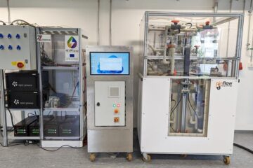
Efficient, sustainable and cost-effective hybrid energy storage system for modern power grids
EU project HyFlow: Over three years of research, the consortium of the EU project HyFlow has successfully developed a highly efficient, sustainable, and cost-effective hybrid energy storage system (HESS) that…

