UW-Madison team invents fast, flexible computer chips on plastic
Historically, the semiconductor industry has relied on flat, two-dimensional chips upon which to grow and etch the thin films of material that become electronic circuits for computers and other electronic devices. But as thin as those chips might seem, they are quite beefy in comparison to the result of a new UW-Madison semiconductor fabrication process detailed in the current issue of the Journal of Applied Physics.
A team led by electrical and computer engineer Zhenqiang (Jack) Ma and materials scientist Max Lagally have developed a process to remove a single-crystal film of semiconductor from the substrate on which it is built. This thin layer (only a couple of hundred nanometers thick) can be transferred to glass, plastic or other flexible materials, opening a wide range of possibilities for flexible electronics. In addition, the semiconductor film can be flipped as it is transferred to its new substrate, making its other side available for more components. This doubles the possible number of devices that can be placed on the film.
By repeating the process, layers of double-sided, thin-film semiconductors can be stacked together, creating powerful, low-power, three-dimensional electronic devices.
“It's important to note that these are single-crystal films of strained silicon or silicon germanium,” says Ma. “Strain is introduced in the way we form the membrane. Introducing strain changes the arrangement of atoms in the crystal such that we can achieve much faster device speed while consuming less power.”
For non-computer applications, flexible electronics are beginning to have significant impact. Solar cells, smart cards, radio frequency identification (RFID) tags, medical applications, and active-matrix flat panel displays could all benefit from the development. The techniques could allow flexible semiconductors to be embedded in fabric to create wearable electronics or computer monitors that roll up like a window shade.
“This is potentially a paradigm shift,” says Lagally. “The ability to create fast, low-power, multilayer electronics has many exciting applications. Silicon germanium membranes are particularly interesting. Germanium has a much higher adsorption for light than silicon. By including the germanium without destroying the quality of the material, we can achieve devices with two to three orders of magnitude more sensitivity.”
That increased sensitivity could be applied to create superior low-light cameras, or smaller cameras with greater resolution.
Media Contact
More Information:
http://www.wisc.eduAll latest news from the category: Physics and Astronomy
This area deals with the fundamental laws and building blocks of nature and how they interact, the properties and the behavior of matter, and research into space and time and their structures.
innovations-report provides in-depth reports and articles on subjects such as astrophysics, laser technologies, nuclear, quantum, particle and solid-state physics, nanotechnologies, planetary research and findings (Mars, Venus) and developments related to the Hubble Telescope.


Newest articles
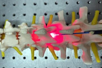
Red light therapy for repairing spinal cord injury passes milestone
Patients with spinal cord injury (SCI) could benefit from a future treatment to repair nerve connections using red and near-infrared light. The method, invented by scientists at the University of…
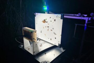
Insect research is revolutionized by technology
New technologies can revolutionise insect research and environmental monitoring. By using DNA, images, sounds and flight patterns analysed by AI, it’s possible to gain new insights into the world of…

X-ray satellite XMM-newton sees ‘space clover’ in a new light
Astronomers have discovered enormous circular radio features of unknown origin around some galaxies. Now, new observations of one dubbed the Cloverleaf suggest it was created by clashing groups of galaxies….

