Lighting the way to better nanoscale films
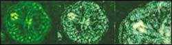
Left: The crystal structure of a thin-film polymer "seaweed" crystal that is about four micrometers wide. Brighter areas indicate parts of the crystal with the greatest "strain." Center: The same crystal with lines superimposed showing the direction of strain between the crystal’s atoms. Right: Closeup of the upper left portion of the center image.
Most miniature electronic, optical and micromechanical devices are made from expensive semiconductor or ceramic materials. For some applications like diagnostic lab-on-a-chip devices, thin-film polymers may provide a cheaper alternative, but the structure and properties of these materials—-often no more than a few nanometers (nm) thick—-are difficult to determine. In addition, defects in the thin polymer masking materials used to “print” integrated circuits can produce malfunctioning components. Consequently, researchers would like to have a non-invasive method for scanning polymer films for defects at high resolution.
In the Aug. 23 issue of Applied Physics Letters,* researchers at the National Institute of Standards and Technology (NIST) report on an application of a new method for studying ultrathin polymers that makes it possible to visualize defects and structure in these materials and should help improve basic understanding of crystal formation in polymers.
Using a special form of near-field scanning optical microscopy, the NIST researchers were able to determine the structure of, and “strain” (stretching between atoms) in, thin-film crystals of polystyrene. Polystyrene is a ubiquitous plastic found in foam cups, CD cases and many other products.
The films examined formed tiny crystals just 15 nm thick and about 1500 nanometers wide, which makes them difficult to study with other optical microscopes. In the NIST experiments, blue-green light was piped through a glass fiber about 50 nm wide and scanned across the sample about 10 nm above the surface. Changes in the polarization of the light (the direction of the wave’s electric field) as it transmits through the sample then were used to investigate the material’s crystal structure and to map areas of strain.
The NIST results should help scientists choose and improve polymer materials and processes for fabricating a range of microscale and nanoscale plastic devices.
Media Contact
More Information:
http://www.nist.govAll latest news from the category: Physics and Astronomy
This area deals with the fundamental laws and building blocks of nature and how they interact, the properties and the behavior of matter, and research into space and time and their structures.
innovations-report provides in-depth reports and articles on subjects such as astrophysics, laser technologies, nuclear, quantum, particle and solid-state physics, nanotechnologies, planetary research and findings (Mars, Venus) and developments related to the Hubble Telescope.


Newest articles

Sea slugs inspire highly stretchable biomedical sensor
USC Viterbi School of Engineering researcher Hangbo Zhao presents findings on highly stretchable and customizable microneedles for application in fields including neuroscience, tissue engineering, and wearable bioelectronics. The revolution in…

Twisting and binding matter waves with photons in a cavity
Precisely measuring the energy states of individual atoms has been a historical challenge for physicists due to atomic recoil. When an atom interacts with a photon, the atom “recoils” in…
Nanotubes, nanoparticles, and antibodies detect tiny amounts of fentanyl
New sensor is six orders of magnitude more sensitive than the next best thing. A research team at Pitt led by Alexander Star, a chemistry professor in the Kenneth P. Dietrich…

